
User's Manual
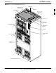
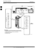
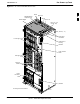
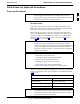
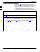
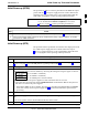
Table Of Contents
- Contents
- Chapter 1 Introduction
- Chapter 2 Preliminary Operations
- Chapter 3 Optimization/Calibration

Initial Power–up Tests and Procedures68P09258A31–A
Oct 2003
1X SCt 4812T BTS Optimization/ATP
2-15
Initial Power-up (RFDS)
The procedure in Table 2-6 must be performed on the RFDS after input
power from the common power supply has been verified. Perform the
following steps to apply initial power to the cards/modules within the
frame itself, verifying that each is operating within specification.
NOTE
Visual inspection of card placement and equipage for each frame
vs. site documentation must be completed, as covered in
Table 2-1, on page 2-3, before proceeding with this test.
Table 2-6: Initial Power-up (RFDS)
Step Action
1 On the RFDS, set the input power rocker switch (P1) to the ON position (see Figure 2-7).
2 Verify power supply output voltages (at the top of BTS frame), using a digital voltmeter, are within
specifications: +27.0 V nominal.
Initial Power-up (BTS)
The procedure must be performed on each frame after input power from
the common power supply has been verified. Follow the steps in
Table 2-7 to apply initial power to the cards/modules within the frame
itself, verifying that each is operating within specification.
Table 2-7: Initial Power–up (BTS)
Step Action
1 At the BTS, set the C–CCP (POWER) power distribution breakers (see Figure 2-3 on page 2-8 or
Figure 2-5 on page 2-10) to the ON position by pushing in the breakers.
2 Insert the C–CCP fan modules. Observe that the fan modules come on line.
3
! CAUTION
Verify the correct power/converter modules by observing the locking/retracting tabs appear as follows:
– (in +27 V BTS C–CCP shelf)
– (in –48 V BTS C–CCP shelf)
– (in –48 V BTS power conversion shelf)
Insert and lock the converter/power supplies into their associated slots one at a time.
• If no boards have been inserted, all three PWR/ALM LEDs would indicate RED to notify the user
that there is no load on the power supplies.
– If the LED is RED, do not be alarmed. After Step 4 is performed, the LEDs should turn GREEN;
if not, then a faulty converter/power supply module is indicated and should be replaced before
proceeding.
STPN 4045A
PWR CONV CDMA RCVR
STPN 4044A
PWR CONV LPA
STPN4009
PWR CONV CDMA RCVR
4 Seat and lock all remaining circuit cards and modules in the C–CCP shelf into their associated slots.
5 Seat the first equipped LPA module pair into the assigned slot in the upper LPA shelf including LPA
fan.
S In +27 V systems, observe that the LPA internal fan comes on line.
6 Repeat step 5 for all remaining LPAs.
. . . continued on next page
2