Preparing the LMF 68P09258A31–A LMF Operating System Installation This section provides information and instructions for installing and updating the LMF software and files. 3 NOTE First Time Installation Sequence: 1. Install Java Runtime Environment (JRE) 2. Install U/WIN K–shell emulator 3. Install LMF application programs 4.
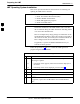
Preparing the LMF 68P09258A31–A Copy BTS and CBSC CDF (or NECF) Files to the LMF Computer Before logging on to a BTS with the LMF computer to execute optimization/ATP procedures, the correct bts-#.cdf (or bts–#.necf) and cbsc-#.cdf files must be obtained from the CBSC and put in a bts-# folder in the LMF computer. This requires creating versions of the CBSC CDF files on a DOS–formatted floppy diskette and using the diskette to install the CDF files on the LMF computer.
Preparing the LMF 68P09258A31–A Table 3-2: Copying CDF or NECF Files to the LMF Computer n Step 7 Action With Solaris versions of Unix, create DOS–formatted versions of the bts-#.cdf (or bts–#.necf) and cbsc-#.cdf files on the diskette by entering the following command: unix2dos /floppy/no_name/ (e.g., unix2dos bts–248.cdf /floppy/no_name/bts–248.cdf). NOTE S Other versions of Unix do not support the unix2dos and dos2unix commands.
Preparing the LMF 68P09258A31–A Creating a Named HyperTerminal Connection for MMI Connection Confirming or changing the configuration data of certain BTS Field Replaceable Units (FRU) requires establishing an MMI communication session between the LMF and the FRU. Using features of the Windows operating system, the connection properties for an MMI session can be saved on the LMF computer as a named Windows HyperTerminal connection.
Preparing the LMF 68P09258A31–A Table 3-3: Creating a Named Hyperlink Connection for MMI Connection Step 3 Action 6 Click OK. 7 Save the defined connection by selecting: File>Save 8 Close the HyperTerminal window by selecting: File>Exit 9 Click Yes to disconnect when prompted. 10 Perform one of the following: S If the Hyperterminal folder window is still open (Win 98) proceed to step 12 S From the Windows Start menu, select Programs > Accessories.
Span Lines – Interface and Isolation 68P09258A31–A Span Lines – Interface and Isolation T1/E1 Span Interface At active sites, the OMC/CBSC must disable the BTS and place it out of service (OOS). DO NOT remove the 50–pin TELCO cable connected to the BTS frame site I/O board J1 connector until the OMC/CBSC has disabled the BTS! NOTE Each frame is equipped with one Site I/O and two Span I/O boards. The Span I/O J1 connector provides connection of 25 pairs of wire. A GLI card can support up to six spans.
Span Lines – Interface and Isolation 68P09258A31–A T1/E1 Span Isolation Table 3-4 describes the action required for span isolation. Table 3-4: T1/E1 Span Isolation Step 3 Action 1 Have the OMC/CBSC place the BTS OOS. 2 The T1/E1 span 50–pin TELCO cable connected to the BTS frame SPAN I/O board J1 connector can be removed from both Span I/O boards, if equipped, to isolate the spans. NOTE If a third party is used for span connectivity, the third party must be informed before disabling the span line.
LMF to BTS Connection 68P09258A31–A LMF to BTS Connection Connect the LMF to the BTS The LMF is connected to the LAN A or B connector located on the left side of the frame’s lower air intake grill, behind the LAN Cable Access door (see Figure 3-3). Table 3-5: LMF to BTS Connection Step Action 1 To gain access to the connectors, open the LAN cable access door, then pull apart the fabric covering the BNC “T” connector (see Figure 3-3).
Using the LMF 68P09258A31–A Using the LMF Basic LMF Operation LMF Coverage in This Publication – The LMF application program supports maintenance of both CDMA and SAS BTSs. All references to the LMF in this publication are to the CDMA portion of the program.
Using the LMF 68P09258A31–A The LMF Display and the BTS BTS Display – When the LMF is logged into a BTS, a frame tab is displayed for each BTS frames. The frame tab will be labeled with “CDMA” and the BTS number, a dash, and the frame number (for example, BTS–812–1 for BTS 812, RFMF 1). If there is only one frame for the BTS, there will only be one tab.
Using the LMF 68P09258A31–A Understanding GUI Operation The following screen captures are provided to help understand how the GUI operates: – Figure 3-4 depicts the differences between packet and circuit CDMA “cdf” file identification. Note that if there is a packet version “bts” file, the “(P)” is added as a suffix. There is a corresponding “(C)” for the circuit mode version. – Figure 3-5 depicts the Self-Managed Network Elements (NEs) state of a packet mode SC4812T.
Using the LMF 68P09258A31–A Figure 3-4: BTS Login screen – identifying circuit and packet BTS files 3 Oct 2003 1X SCt 4812T BTS Optimization/ATP 3-21
Using the LMF 68P09258A31–A Figure 3-5: Self–Managed Network Elements (NEs) state of a packet mode SC4812T 3 3-22 1X SCt 4812T BTS Optimization/ATP Oct 2003
Using the LMF 68P09258A31–A Figure 3-6: Available packet mode commands 3 Oct 2003 1X SCt 4812T BTS Optimization/ATP 3-23
Using the LMF 68P09258A31–A Figure 3-7: Packet mode site with MCC–1 and BBX–1 under LMF control 3 3-24 1X SCt 4812T BTS Optimization/ATP Oct 2003
Using the LMF 68P09258A31–A Command Line Interface Overview The LMF also provides Command Line Interface (CLI) capability. Activate the CLI by clicking on a shortcut icon on the desktop. The CLI can not be launched from the GUI, only from the desktop icon. Both the GUI and the CLI use a program known as the handler. Only one handler can be running at one time. Due to architectural limitations, the GUI must be started before the CLI if you want the GUI and CLI to use the same handler.
Using the LMF 68P09258A31–A Logging into a BTS Logging into a BTS establishes a communication link between the BTS and the LMF. An LMF session can be logged into only one BTS at a time. Prerequisites Before attempting to log into a BTS, ensure the following have been completed: S The LMF is correctly installed on the LMF computer. S A bts-nnn folder with the correct CDF/NECF and CBSC files exists.
Using the LMF 68P09258A31–A Table 3-6: BTS GUI Login Procedure n Step Action NOTE 128.0.0.2 is the default IP address for MGLI–1 in field BTS units. 128.0.0.1 is the default IP address for MGLI–2. 7 Type in the correct IP Port number (normally 9216) if not correctly displayed in the IP Port box. 8 Click on Ping. – If the connection is successful, the Ping Display window shows text similar to the following: 3 Reply from 128 128.0.0.
Using the LMF 68P09258A31–A BTS Login from the CLI Environment Follow the procedure in Table 3-7 to log into a BTS when using the CLI environment. NOTE If the CLI and GUI environments are to be used at the same time, the GUI must be started first and BTS login must be performed from the GUI. Refer to Table 3-6 to start the GUI environment and log into a BTS.
Using the LMF 68P09258A31–A Logging Out Logging out of a BTS is accomplished differently for the GUI and CLI operating environments. NOTE The GUI and CLI environments use the same connection to a BTS. If a GUI and the CLI session are running for the same BTS at the same time, logging out of the BTS in either environment will log out of it for both. When either a login or logout is performed in the CLI window, there is no GUI indication that the login or logout has occurred.
Using the LMF 68P09258A31–A Logging Out of a BTS from the CLI Environment Follow the procedure in Table 3-9 to logout of a BTS when using the CLI environment. Table 3-9: BTS CLI Logout Procedure n Step Action NOTE If the BTS is also logged into from a GUI running at the same time and further work must be done with it in the GUI, proceed to Step 2. 1 3 Log out of a BTS by entering the following command: logout bts– A response similar to the following will be displayed: LMF> 13:24:51.
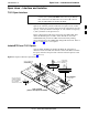
Using the LMF 68P09258A31–A Establishing an MMI Communication Session Equipment Connection – Figure 3-8 illustrates common equipment connections for the LMF computer. For specific connection locations on FRUs, refer to the illustration accompanying the procedures which require the MMI communication session. Initiate MMI Communication – For those procedures which require MMI communication between the LMF and BTS FRUs, follow the procedures in Table 3-10 to initiate the communication session.
Using the LMF 68P09258A31–A Figure 3-8: CDMA LMF Computer Common MMI Connections To FRU MMI port 8–PIN NULL MODEM BOARD (TRN9666A) 8–PIN TO 10–PIN RS–232 CABLE (P/N 30–09786R01) 3 LMF COMPUTER RS–232 CABLE COM1 OR COM2 DB9–TO–DB25 ADAPTER FW00687 Online Help Task oriented online help is available in the LMF by clicking on Help in the window menu bar, and selecting LMF Help from the pull–down menu.
Pinging the Processors 68P09258A31–A Pinging the Processors Pinging the BTS For proper operation, the integrity of the Ethernet LAN A and B links must be be verified. Figure 3-9 represents a typical BTS Ethernet configuration. The drawing depicts one link (of two identical links), A and B. Ping is a program that routes request packets to the LAN network modules to obtain a response from the specified “targeted” BTS.
Pinging the Processors 68P09258A31–A NOTE IMPORTANT: The Ethernet LAN A and B cables must be installed on each frame/enclosure before performing this test. All other processor board LAN connections are made via the backplanes. Table 3-11: Pinging the Processors n Step 3 Action 1 If you have not already done so, connect the LMF to the BTS (see Table 3-5 on page 3-17). 2 From the Windows desktop, click the Start button and select Run.
Download the BTS 68P09258A31–A Download the BTS Overview Before a BTS can operate, each equipped device must contain device initialization (ROM) code. ROM code is loaded in all devices during manufacture or factory repair, or, for software upgrades, from the CBSC using the DownLoad Manager (DLM). Device application (RAM) code and data must be downloaded to each equipped device by the user before the BTS can be made fully functional for the site where it is installed.
Download the BTS 68P09258A31–A When code is downloaded to an MGLI or GLI, the LMF automatically also downloads data and then enables the MGLI. When enabled, the MGLI will change to INS_ACT (bright green). A redundant GLI will not be automatically enabled and will remain OOS_RAM (yellow). When the redundant GLI is manually commanded to enable through the LMF, it will change state to INS_SBY (olive green). For non–MGLI devices, data must be downloaded after RAM code is downloaded.
Download the BTS 68P09258A31–A Verify GLI ROM Code Loads Devices should not be loaded with a RAM code version which is not compatible with the ROM code with which they are loaded. Before downloading RAM code and data to the processor cards, follow the procedure in Table 3-12 to verify the GLI devices are loaded with the correct ROM code for the software release used by the BSS.
Download the BTS 68P09258A31–A Download RAM Code and Data to MGLI and GLI Follow the procedure in Table 3-13 to download the firmware application code for the MGLI. The download code action downloads data and also enables the MGLI. Prerequisite S Prior to performing this procedure, ensure a code file exists for each of the devices to be loaded. S The LMF computer is connected to the BTS (refer to Table 3-5), and is logged in using the GUI environment (refer to Table 3-6).
Download the BTS 68P09258A31–A Download Code and Data to Non–GLI Devices Downloads to non–GLI devices can be performed individually for each device or all equipped devices can be downloaded with one action. NOTE – When downloading multiple devices, the download may fail for some of the devices (a time out occurs). These devices can be downloaded separately after completing the multiple download. – CSM devices are RAM code–loaded at the factory.
Download the BTS 68P09258A31–A Select CSM Clock Source CSMs must be enabled prior to enabling the MCCs. Procedures in the following two sub-sections cover the actions to accomplish this. For additional information on the CSM sub–system, see “Clock Synchronization Manager (CSM) Sub–system Description” in the CSM System Time – GPS & LFR/HSO Verification section of this chapter. Select CSM Clock Source A CSM can have three different clock sources.
Download the BTS 68P09258A31–A Enable CSMs NOTE – CSMs are code loaded at the factory. This data is retained in EEPROM. The download code procedure is required in the event it becomes necessary to code load CSMs with updated software versions. Use the status function to determine the current code load versions. – The CSM(s) to be enabled must have been downloaded with code (Yellow, OOS–RAM) and data. Each BTS CSM system features two CSM boards per site.
Download the BTS 68P09258A31–A Table 3-16: Enable CSMs n Step Action NOTE – If equipped with two CSMs, CSM–1 should be bright green (INS–ACT) and CSM–2 should be dark green (INS–STY) – After the CSMs have been successfully enabled, observe the PWR/ALM LEDs are steady green (alternating green/red indicates the card is in an alarm state). 3 If more than an hour has passed, refer to CSM Verification, see Figure 3-11 and Table 3-20 to determine the cause.
68P09258A31–A CSM System Time – GPS & LFR/HSO Verification CSM System Time – GPS & LFR/HSO Verification CSM & LFR Background The primary function of the Clock Synchronization Manager (CSM) boards (slots 1 and 2) is to maintain CDMA system time. The CSM in slot 1 is the primary timing source while slot 2 provides redundancy. The CSM2 card (CSM second generation) is required when using the remote GPS receiver (R–GPS). R–GPS uses a GPS receiver in the antenna head that has a digital output to the CSM2 card.
CSM System Time – GPS & LFR/HSO Verification 68P09258A31–A Low Frequency Receiver/High Stability Oscillator (LFR/HSO) The CSM and the LFR/HSO – The CSM performs the overall configuration and status monitoring functions for the LFR/HSO. In the event of GPS failure, the LFR/HSO is capable of maintaining synchronization initially established by the GPS reference signal. LFR – The LFR requires an active external antenna to receive LORAN–C RF signals.
CSM System Time – GPS & LFR/HSO Verification 68P09258A31–A CSM Frequency Verification The objective of this procedure is the initial verification of the CSM boards before performing the RF path verification tests. Parts of this procedure will be repeated for final verification after the overall optimization has been completed. Null Modem Cable A null modem cable is required. It is connected between the MMI port of the primary CSM and the null modem board.
CSM System Time – GPS & LFR/HSO Verification 68P09258A31–A Test Equipment Setup: GPS & LFR/HSO Verification Follow the procedure in Table 3-19 to set up test equipment while referring to Figure 3-11 as required. Table 3-19: Test Equipment Setup (GPS & LFR/HSO Verification) Step 1 Action Perform one of the following operations: S For local GPS (RF–GPS), verify a CSM board with a GPS receiver is installed in primary CSM slot 1 and that CSM–1 is INS.
CSM System Time – GPS & LFR/HSO Verification 68P09258A31–A Figure 3-11: CSM MMI terminal connection REFERENCE OSCILLATOR CSM board shown removed from frame MMI SERIAL PORT 3 EVEN SECOND TICK TEST POINT REFERENCE GPS RECEIVER ANTENNA INPUT ANTENNA COAX CABLE GPS RECEIVER 19.6 MHZ TEST POINT REFERENCE (NOTE 1) NULL MODEM BOARD (TRN9666A) 9–PIN TO 9–PIN RS–232 CABLE FW00372 LMF NOTEBOOK DB9–TO–DB25 ADAPTER COM1 NOTES: 1.
CSM System Time – GPS & LFR/HSO Verification 68P09258A31–A GPS Initialization/Verification Follow the procedure in Table 3-20 to initialize and verify proper GPS receiver operation. Prerequisites Ensure the following prerequisites have been met before proceeding: S The LMF is not logged into the BTS. S The COM1 port is connected to the MMI port of the primary CSM via a null modem board (see Figure 3-11). 3 S The primary CSM and HSO (if equipped) have been warmed up for at least 15 minutes.
68P09258A31–A CSM System Time – GPS & LFR/HSO Verification Table 3-20: GPS Initialization/Verification Step Action 1 To verify that Clock alarms (0000), Dpll is locked and has a reference source, and GPS self test passed messages are displayed within the report, issue the following MMI command bstatus – Observe the following typical response: Clock Alarms (0000): DPLL is locked and has a reference source.
CSM System Time – GPS & LFR/HSO Verification 68P09258A31–A Table 3-20: GPS Initialization/Verification Step 3 Action 4 If any of the above mentioned areas fail, verify: – If LED is RED, verify that HSO had been powered up for at least 5 minutes.
68P09258A31–A CSM System Time – GPS & LFR/HSO Verification Table 3-20: GPS Initialization/Verification Step Action 7 Verify the following GPS information (shown above in underlined text): – At least 4 satellites are tracked, and 4 satellites are visible. – GPS Receiver Control Task State is “tracking satellites”. Do not continue until this occurs! – Dilution of Precision indication is not more that 30.
CSM System Time – GPS & LFR/HSO Verification 68P09258A31–A Table 3-20: GPS Initialization/Verification Step 10 Action Observe the following typical response if the CSM is warmed up.
CSM System Time – GPS & LFR/HSO Verification 68P09258A31–A Table 3-21: LFR Initialization/Verification Step Action 1 At the CSM> prompt, enter lstatus to verify that the LFR is in tracking mode.
CSM System Time – GPS & LFR/HSO Verification 68P09258A31–A Table 3-21: LFR Initialization/Verification Step 4 Action Note LORAN–C LFR information (highlighted above in boldface type) is usually the #1 reference source (verified from left to right). NOTE If any of the above mentioned areas fail, verify: – The LFR antenna is not obstructed or misaligned. – The antenna pre–amplifier power and calibration twisted pair connections are intact and < 91.4 m (300 ft) in length.
68P09258A31–A CSM System Time – GPS & LFR/HSO Verification Prerequisites S The LMF is not logged into the BTS. S The COM1 port is connected to the MMI port of the primary CSM via a null modem board. S The primary CSM and the HSO (if equipped) have warmed up for 15 minutes. If the BTS is equipped with an HSO, follow the procedure in Table 3-22 to configure the HSO. Table 3-22: HSO Initialization/Verification Step 1 3 Action At the BTS, slide the HSO card into the cage.
Test Equipment Set-up 68P09258A31–A Test Equipment Set-up Connecting Test Equipment to the BTS The following equipment is required to perform optimization: S S S S S S 3 LMF Test set Directional coupler and attenuator RF cables and connectors Null modem cable (see Figure 3-10) GPIB interface box Refer to Table 3-23 and Table 3-24 for an overview of connections for test equipment currently supported by the LMF.
Test Equipment Set-up 68P09258A31–A Supported Test Equipment CAUTION To prevent damage to the test equipment, all TX test connections must be through the directional coupler and in-line attenuator as shown in the test setup illustrations.
Test Equipment Set-up 68P09258A31–A Test Equipment Connection Charts To use the following charts to identify necessary test equipment connections, locate the communications system analyzer being used in the COMMUNICATIONS SYSTEM ANALYZER columns, and read down the column. Where a dot appears in the column, connect one end of the test cable to that connector. Follow the horizontal line to locate the end connection(s), reading up the column to identify the appropriate equipment and/or BTS connector.
Test Equipment Set-up 68P09258A31–A CDMA2000 1X/IS–95A/B–capable Test Equipment Connections Table 3-24 depicts the interconnection requirements for currently available test equipment supporting both CDMA 2000 1X and IS–95A/B which meets Motorola standards and is supported by the LMF. Table 3-24: CDMA2000 1X/IS–95A/B Test Equipment Interconnection COMMUNICATIONS SYSTEM ANALYZER SIGNAL EVEN SECOND SYNCHRONIZATION 19.
Test Equipment Set-up 68P09258A31–A Equipment Warm-up 3 NOTE To assure BTS stability and contribute to optimization accuracy of the BTS, warm-up the BTS test equipment prior to performing the BTS optimization procedure as follows: – Agilent E7495A for a minimum of 30 minutes – All other test sets for a minimum of 60 minutes Time spent running initial or normal power-up, hardware/ firmware audit, and BTS download counts as warm-up time.
Test Equipment Set-up 68P09258A31–A Figure 3-12: IS–95A/B Cable Calibration Test Setup – CyberTest, Agilent 8935, Advantest R3465, and HP 8921A SUPPORTED TEST SETS CALIBRATION SET UP Motorola CyberTest A. SHORT CABLE CAL ÎÎÎ ÎÎÎÏ SHORT CABLE TEST SET 3 ANT IN RF GEN OUT Note: The Directional Coupler is not used with the Cybertest Test Set. The TX cable is connected directly to the Cybertest Test Set. B.
Test Equipment Set-up 68P09258A31–A Figure 3-13: IS–95A/B and CDMA 2000 1X Cable Calibration Test Setup – Agilent E4406A/E4432B and Advantest R3267/R3562 SUPPORTED TEST SETS CALIBRATION SET UP A. SHORT CABLE CAL Agilent E4432B (Top) and E4406A (Bottom) SHORT CABLE TEST SET RF OUTPUT 50 OHM 3 B. RX TEST SETUP RF INPUT 50 OHM N–N FEMALE ADAPTER Advantest R3267 (Top) and R3562 (Bottom) RX CABLE SHORT CABLE TEST SET RF IN EXT TRIG IN MOD TIME BASE IN (EXT REF IN) RF OUT C.
Test Equipment Set-up 68P09258A31–A Figure 3-14: CDMA2000 1X Cable Calibration Test Setup – Agilent 8935/E4432B CALIBRATION SET UP SUPPORTED TEST SETS A. SHORT CABLE CAL Agilent E4432B (Top) and 8935 Series E6380A (Bottom) SHORT CABLE TEST SET 3 ÁÁ Á ÁÁÁ RF OUTPUT 50 Ω B. RX TEST SETUP N–N FEMALE ADAPTER RX CABLE ANT IN SHORT CABLE NOTE: TEST SET 10 MHZ IN ON REAR OF SIGNAL GENERATOR IS CONNECTED TO 10 MHZ REF OUT ON SIDE OF CDMA BASE STATION TEST SET. D. TX TEST SETUP 50 Ω ΤERM.
Test Equipment Set-up 68P09258A31–A Figure 3-15: CDMA2000 1X Cable Calibration Test Setup – Agilent E7495A SUPPORTED TEST SETS Agilent E7495A CALIBRATION SET UP A. SHORT CABLE CAL 10 DB PAD SHORT CABLE TEST SET 10 DB PAD 3 D. RX and TX TEST SETUP 50 Ω ΤERM.
Test Equipment Set-up 68P09258A31–A Set-up for TX Calibration Figure 3-16 through Figure 3-18 show the test set connections for TX calibration. Figure 3-16: TX Calibration Test Setup – CyberTest (IS–95A/B) and Agilent 8935 (IS–95A/B and CDMA2000 1X), and Advantest R3465 TEST SETS TRANSMIT (TX) SET UP Motorola CyberTest POWER SENSOR 100–WATT (MIN) NON–RADIATING RF LOAD ÎÎÎÎ ÎÎÎÎÏ FRONT PANEL 3 OUT 2O DB PAD (FOR 1.7/1.9 GHZ) NOTE: THE DIRECTIONAL COUPLER IS NOT USED WITH THE CYBERTEST TEST SET.
Test Equipment Set-up 68P09258A31–A Figure 3-17: TX Calibration Test Setup – Agilent E4406A and Advantest R3567 (IS–95A/B and CDMA2000 1X) TEST SETS TRANSMIT (TX) SET UP Advantest Model R3267 POWER SENSOR 100–WATT (MIN) NON–RADIATING RF LOAD POWER METER (OPTIONAL)* OUT 3 2O DB PAD (FOR 1.7/1.
Test Equipment Set-up 68P09258A31–A Figure 3-18: TX Calibration Test Setup – Agilent E7495A (IS–95A/B and CDMA2000 1X) TEST SETS TRANSMIT (TX) SET UP Agilent E7495A POWER SENSOR NOTE: IF BTS IS EQUIPPED WITH DUPLEXED RX/TX SIGNALS, CONNECT THE TX TEST CABLE TO THE DUPLEXED ANTENNA CONNECTOR. POWER METER PORT 1 RF OUT COMMUNICATIONS SYSTEM ANALYZER 100–WATT (MIN.) NON–RADIATING RF LOAD PORT 2 RF IN INTERNAL ETHERNET CARD TX TEST CABLE 3 DIRECTIONAL COUPLER (30 DB) 50 Ω TERM .
Test Equipment Set-up 68P09258A31–A Setup for Optimization/ATP Figure 3-19 and Figure 3-21 show test set connections for IS–95 A/B optimization/ATP tests. Figure 3-21 and Figure 3-22 show test set connections for IS-95 A/B/C optimization/ATP tests. Figure 3-19: Optimization/ATP Test Setup Calibration – Agilent 8935 TEST SET Optimization/ATP SET UP Agilent 8935 Series E6380A (formerly HP 8935) 3 SYNC MONITOR EVEN SEC TICK PULSE REFERENCE FROM CSM BOARD FREQ MONITOR 19.
Test Equipment Set-up 68P09258A31–A Figure 3-20: Optimization/ATP Test Setup – HP 8921 TEST SETS Optimization/ATP SET UP Hewlett–Packard Model HP 8921A W/PCS Interface (for 1700 and 1900 MHz) SYNC MONITOR EVEN SEC TICK PULSE REFERENCE FROM CSM BOARD FREQ MONITOR 19.6608 MHZ CLOCK REFERENCE FROM CSM BOARD NOTE: IF BTS RX/TX SIGNALS ARE DUPLEXED (4800E): BOTH THE TX AND RX TEST CABLES CONNECT TO THE DUPLEXED ANTENNA GROUP.
Test Equipment Set-up 68P09258A31–A Figure 3-21: IS–95A/B and CDMA2000 1X Optimization/ATP Test Setup – Advantest R3267/3562, Agilent E4432B/E4406A TEST SETS Optimization/ATP SET UP Advantest R3267 (Top) and R3562 (Bottom) TO EXT TRIG ON REAR OF SPECTRUM ANALYZER 10 MHZ REF OUT NOTE: IF BTS RX/TX SIGNALS ARE DUPLEXED: BOTH THE TX AND RX TEST CABLES CONNECT TO THE DUPLEXED ANTENNA GROUP. BASEBAND GEN. REF.
Test Equipment Set-up 68P09258A31–A Figure 3-22: IS–95A/B and CDMA2000 1X Optimization/ATP Test Setup – Agilent E7495A ATP TEST SET UP TEST SET POWER METER Agilent E7495A NOTE: IF BTS IS EQUIPPED WITH DUPLEXED RX/TX SIGNALS, CONNECT THE TX TEST CABLE TO THE DUPLEXED ANTENNA CONNECTOR. RX TEST RF INPUT 50 Ω OR INPUT 50 Ω 100–WATT (MIN.
Test Equipment Set-up 68P09258A31–A ATP Setup with Directional Couplers Figure 3-23 shows a typical TX ATP setup.
Test Equipment Set-up 68P09258A31–A Figure 3-24: Typical RX ATP Setup with Directional Coupler Figure 3-24 shows a typical RX ATP setup. COBRA RFDS Detail RX ANTENNA DIRECTIONAL COUPLERS RX RF FROM BTS FRAME 2 3 4 5 6 RX (RFM TX) 1 TX (RFM RX) RFDS TX (RFM RX) COUPLER OUTPUTS TO RFDS FWD(BTS) ASU1 (SHADED) CONNECTORS 3 RF FEED LINE TO TX ANTENNA REMOVED Connect RX test cable between the test set and the appropriate RX antenna directional coupler.
Test Set Calibration 68P09258A31–A Test Set Calibration Background Proper test equipment calibration ensures that the test equipment and associated test cables do not introduce measurement errors, and that measurements are correct. NOTE If the test equipment set being used to optimize or test the BTS has been calibrated and maintained as a set, this procedure does not need to be performed. This procedure must be performed prior to beginning the optimization.
Test Set Calibration 68P09258A31–A Cable Calibration – Manual cable calibration procedures using the HP 8921A and Advantest R3465 communications system analyzers are provided in the Manual Cable Calibration section of Appendix F, if needed. GPIB Addresses GPIB addresses can range from 1 through 30. The LMF will accept any address in that range, but the numbers entered in the LMF Options window GPIB address box must match the addresses of the test equipment.
Test Set Calibration 68P09258A31–A Manually Selecting Test Equipment in a Serial Connection Tab Test equipment can be manually specified before, or after, the test equipment is connected. The LMF does not check to see if the test equipment is actually detected for manual specification. Follow the procedure in Table 3-25 to select test equipment manually.
Test Set Calibration 68P09258A31–A Automatically Selecting Test Equipment in Serial Connection Tab When using the auto-detection feature to select test equipment, the LMF examines which test equipment items are actually communicating with the LMF. Follow the procedure in Table 3-26 to use the auto-detection feature. Table 3-26: Selecting Test Equipment Using Auto-Detect n Step Action 1 In the LMF window menu bar, click Tools and select Options... from the pull–down menu. The LMF Options window appears.
Test Set Calibration 68P09258A31–A Calibrating Test Equipment The calibrate test equipment function zeros the power measurement level of the test equipment item that is to be used for TX calibration and audit. If both a power meter and an analyzer are connected, only the power meter is zeroed. NOTE The Agilent E4406A transmitter tester does not support power measurement level zeroing. Refer to the Equipment Calibration section of Appendix F for E4406A calibration.
Test Set Calibration 68P09258A31–A Calibrating Cables Overview The LMF Cable Calibration function is used to measure the path loss (in dB) for the TX and RX cables, adapters, directional couplers, and attenuators that make up the cable configurations used for testing. A communications system analyzer is used to measure the loss of both the TX test cable and the RX test cable configurations.
Test Set Calibration 68P09258A31–A Calibrate Test Cabling using Communications System Analyzer Cable Calibration is used to calibrate both TX and RX test cables. Appendix F covers the procedures for manual cable calibration. NOTE 3 LMF cable calibration cannot be accomplished using an HP8921 analyzer for 1.7/1.9 GHz. A different analyzer type or the signal generator and spectrum analyzer method (Table 3-29 and Figure 3-25) must be used.
Test Set Calibration 68P09258A31–A Calibrate Test Cabling Using Signal Generator & Spectrum Analyzer Follow the procedure in Table 3-29 to calibrate the TX/Duplexed RX cables using a signal generator and spectrum analyzer. Refer to Figure 3-25, if required. Follow the procedure in Table 3-30 to calibrate the Non–Duplexed RX cables using the signal generator and spectrum analyzer. Refer to Figure 3-26, if required.
Test Set Calibration 68P09258A31–A Table 3-30: Calibrating Non–Duplexed RX Cables Using a Signal Generator &Spectrum Analyzer Step Action NOTE When preparing to calibrate a BTS with Duplexed TX and RX the RX cable calibration must be done using calibration setup in Figure 3-25 and the procedure in Table 3-29. 3 1 Connect a short test cable between the spectrum analyzer and the signal generator as shown in Figure 3-26, detail “A” (top portion of figure).
Test Set Calibration 68P09258A31–A Setting Cable Loss Values Cable loss values for TX and RX test cable configurations are normally set by accomplishing automatic cable calibration using the LMF and the applicable test equipment. The LMF stores the measured loss values in the cable loss files. The cable loss values can also be set or changed manually. Follow the procedure in Table 3-31 to set cable loss values.
Test Set Calibration 68P09258A31–A Setting TX Coupler Loss Values If an in–service TX coupler is installed, the coupler loss (e.g., 30 dB) must be manually entered so it will be included in the LMF TX calibration and audit calculations and RX FER Test. Follow the procedure in Table 3-32 to set coupler loss values.
Bay Level Offset Calibration 68P09258A31–A Bay Level Offset Calibration Introduction Bay Level Offset (BLO) calibration is the central activity of the optimization process. BLO calibration compensates for normal equipment variations within the BTS RF paths and assures the correct transmit power is available at the BTS antenna connectors to meet site performance requirements.
Bay Level Offset Calibration 68P09258A31–A TX Path Calibration The TX Path Calibration assures correct site installation, cabling, and the first order functionality of all installed equipment. The proper function of each RF path is verified during calibration. The external test equipment is used to validate/calibrate the TX paths of the BTS. WARNING Before installing any test equipment directly to any TX OUT connector you must first verify that there are no CDMA channels keyed.
Bay Level Offset Calibration 68P09258A31–A S The calibration data for a BBX is organized as a large flat array. The array is organized by branch, sector, and calibration point. – The first breakdown of the array indicates which branch the contained calibration points are for. The array covers transmit, main receive and diversity receive offsets as follows: Table 3-33: BLO BTS.
Bay Level Offset Calibration 68P09258A31–A Table 3-34: BTS.