BTS Equipment Identification NOTE – continued 1. Figure 1-17 identifies which BBXs are used for Omni and 2-Sector configurations. 2. The fourth PA quadrant (quadrant D) is populated with CLPAs only when the 4x4 ETM is used. 3. PHYSICAL APPEARANCE OF FRAMES: The physical appearance of the frame, especially the location of the MCM, Power Amplifier cage, and Power Distribution/Combiner cage, and the particular I/O plate used, may differ on frames converted from early version SC4812T BTSs.
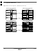
BTS Equipment Identification – continued 1 Figure 1-19: TX Filter and 50Ω Termination Requirements for Omni, Two–sector, and Three–sector Configurations – OEM Multicarrier and Converted Multicarrier Frames (Minimum Power Configuration Shown) Omni CLPA 1A MCM 1 Two–Sector CLPA 1B CLPA 1A 50W TERMINATORS MCM 1 S3 S3 S2 S2 S1 S1 CLPA 1C CLPA 1C CLPA 1B 50W TERMINATOR CLPA 1D TX FILTERS TX FILTER Three–Sector CLPA 1A MCM 1 CLPA 1B S3 S2 TX FILTERS S1 CLPA 1C 5/21/04 1X SC4812T–MC B
1 BTS Equipment Identification – continued Figure 1-20: Omni, Two–sector, and Three–sector PA Configurations – OEM Multicarrier Frame Minimum Power Configuration 3 x 3 ETM CLPA 1A MCM 1 Minimum Power Configuration 4 x 4 ETM CLPA 1B CLPA 1A 50 W TERMINATIONS and/or TX Filters (See NO TAG) S3 S2 S1 CLPA 1C MCM 1 CLPA 2A CLPA 3A CLPA 1B CLPA 3B S2 CLPA 4A S1 CLPA 1A S1 CLPA 4B CLPA 1D MCM 1 CLPA 2A 50 W TERMINATIONS and/or TX Filters (See NO TAG) CLPA 1C CLPA 3A CLPA 4A CLPA 2C CLPA
BTS Equipment Identification – continued 1 Figure 1-21: Omni, Two–sector, and Three–sector PA Configurations – Converted Multicarrier Frame Minimum Power Configuration 3 x 3 ETM CLPA 1A MCM 1 Minimum Power Configuration 4 x 4 ETM CLPA 1B CLPA 1A 50 W TERMINATIONS and/or TX Filters (See NO TAG) S3 S2 S1 CLPA 1C MCM 1 CLPA 2A CLPA 3A S2 S1 CLPA 1B S1 CLPA 1A CLPA 3B CLPA 1D MCM 1 CLPA 2A 50 W TERMINATIONS and/or TX Filters (See NO TAG) CLPA 1C CLPA 3A CLPA 3C 1X SC4812T–MC BTS Optimiza
1 BTS Equipment Identification – continued Figure 1-22: Six–sector PA Configurations – OEM Multicarrier Frames Only Minimum Power Configuration 4 x 4 ETM Minimum Power Configuration 3 x 3 ETM CLPA 1A CLPA 3A MCM 1 S3 CLPA 1B CLPA 1A CLPA 3B CLPA 3A TX FILTERS S2 CLPA 3C CLPA 1C MCM 2 CLPA 3C S6 TX FILTERS CLPA 3A CLPA 1B CLPA 1C CLPA 1A S1 CLPA 3A TX FILTERS CLPA 4B CLPA 1C MCM 2 S5 CLPA 4C 1-42 CLPA 2B S3 S1 MCM 2 CLPA 3C TX FILTERS 1X SC4812T–MC BTS Optimization/ATP D
Chapter 2: Preliminary Operations Table of Contents 5/21/04 Guide Book . . . . . . . . . . . . . . . . . . . . . . . . . . . . . . . . . . . . . . . . . . . . . . . . . . . . . 1–2 Document Overview . . . . . . . . . . . . . . . . . . . . . . . . . . . . . . . . . . . . . . . . . . . . . . What Is In This Guide? . . . . . . . . . . . . . . . . . . . . . . . . . . . . . . . . . . . . . 1–2 1–2 Book Catalogs and Organization . . . . . . . . . . . . . . . . . . . . . . . . . . . . . . . . . . . .
Table of Contents – continued Notes 2 1X SC4812T–MC BTS Optimization/ATP DRAFT 5/21/04
Overview Introduction This section first verifies proper frame equipage. This includes verifying module placement, jumper, and dual in–line package (DIP) switch settings against the site-specific documentation supplied for each BTS application. Next, pre-power up and initial power-up procedures are presented. Cell Site Types Sites are configured as Omni with a maximum of 4 carriers, 3–sectored with a maximum of 4 carriers, and 6–sectored with a maximum of 2 carriers.
Overview – continued Initial Installation of Boards/Modules Follow the procedure in Table 2-1 to verify the initial installation of boards/modules. 2 Table 2-1: Initial Installation of Boards/Modules Step 1 Action Refer to the site documentation and install all boards and modules into the appropriate shelves as required. Verify they are NOT SEATED at this time. NOTE The Switch Card has a configuration switch that must match the site configuration (see Figure 2-1).
Overview – continued Figure 2-1: Switch Card 2 SHIELDS J1 J2 J3 Switch Card J4 J5 Configuration Switch 1 2 3 4 BTS MF ON 3 Sector 6 Sector ti-CDMA-WP-00039-v01-ildoc-ftw Setting Frame C–CCP Shelf Configuration Switch The backplane switch settings behind the fan module nearest the breaker panel should be set as shown in Figure 2-2. The switch setting must be verified and set before power is applied to the BTS equipment.
Overview – continued Figure 2-2: Backplane DIP Switch Settings ALL SWITCHES ON (UP) EXPANSION FRAME SETTING SPEED CONTROLLED FAN MODULE REAR REAR FRONT MODEM_FRAME_ID_0 PWR/ALM AMR / MACH GLI–1 MCC–1 MCC–2 MCC–3 MCC–4 MCC–5 MCC–6 BBX–1 BBX–2 BBX–3 BBX–4 BBX–5 BBX–6 BBX–R MPC AMR / MACH GLI–2 MCC–7 MCC–8 MCC–9 MCC–10 MCC–11 MCC–12 BBX–7 BBX–8 BBX–9 BBX–10 BBX–11 BBX–12 Switch 39 mm Filter Panel CSM CCD CSM HSO CCD MCIO Power Supply Power Supply Power Supply 19 mm Filter Panel FAN MODULE
Pre–Power Up Tests Objective This procedure checks for any electrical short circuits and verifies the operation and tolerances of the cellsite and BTS power supply units prior to applying power for the first time. Test Equipment The following test equipment is required to complete the pre–power–up tests: S Digital Multimeter (DMM) CAUTION Always wear a conductive, high impedance wrist strap while handling the any circuit card/module to prevent damage by ESD.
Pre–Power Up Tests – continued Table 2-2: DC Power Pre–test (BTS Frame) 2 Step 3 Action For –48 V configurations ONLY: Verify the resistance on the –48 V bus: – Remove the Power Supply Modules (PSMs). – Verify that the resistance from the power (–) feed terminal with respect to the ground terminal on the top of the frame measures > 500 Ω (see Figure 2-3). Verify the resistance on the +27 V bus: – Remove PSM#1 or the filler panel. ! CAUTION Do not put probes inside Elcon connectors.
Pre–Power Up Tests – continued Table 2-2: DC Power Pre–test (BTS Frame) Step 8 Action 2 Set the LPA breakers ON by pushing them in. Repeat Step 3 (for –48 V) or Step 4 (for +27 V) after turning on each breaker. – A typical response is that the ohmmeter will steadily climb in resistance as capacitors charge, stopping at approximately 500 Ω.. NOTE Engage circuit breakers only for LPAs that are equipped. 9 In the –48V BTS, insert PSMs one at a time in their associated slots, verifying that LED is green.
Pre–Power Up Tests – continued Figure 2-3: +27V Breaker Panel (–48V is similar) TOP OF FRAME 2 DC FILTER 1 DC FILTER 2 GND 2-4 50 3A 50 4A 1B 50 2B 3B 50 4B 1C 50 2C 3C 50 4C 1D 50 2D 3D 50 4D 1 2 50 2A 3 50 1A 50 INPUT CONNECTOR/ DC FILTER FILLER PLATE L P A ti-CDMA-WP-00224-v01-ildoc-ftw C C C P 1X SC4812T–MC BTS Optimization/ATP DRAFT 5/21/04
Initial Power Up Tests & Procedures Power-up Procedures 2 WARNING Potentially lethal voltage and current levels are routed to the BTS equipment. This test must be performed with a second person present, acting in a safety role. Remove all rings, jewelry, and wrist watches prior to beginning this test. DC Input Power In the tests to follow, power will first be verified at the input to each BTS frame.
Initial Power Up Tests & Procedures – continued Common Power Supply Verification The procedure in Table 2-4 must be performed on any BTS frame connected to a common power supply at the site after the common power supply has been installed and verified per the power supply OEM suggested procedures. 2 Perform the following steps to verify the power input is within specification before powering up the individual cards/modules with the frames themselves.
Initial Power Up Tests & Procedures – continued Table 2-5: Initial Power–up (BTS) Step Action 1 At the BTS, set the C–CCP (POWER) power distribution breakers (see Figure 2-3) to the ON position by pushing in the breakers. 2 Insert the C–CCP fan modules. Observe that the fan modules come on line.
Initial Power Up Tests & Procedures – continued Notes 2 2-8 1X SC4812T–MC BTS Optimization/ATP DRAFT 5/21/04
Chapter 3: Optimization and Calibration Table of Contents 3 5/21/04 Guide Book . . . . . . . . . . . . . . . . . . . . . . . . . . . . . . . . . . . . . . . . . . . . . . . . . . . . . 1–2 Document Overview . . . . . . . . . . . . . . . . . . . . . . . . . . . . . . . . . . . . . . . . . . . . . . What Is In This Guide? . . . . . . . . . . . . . . . . . . . . . . . . . . . . . . . . . . . . . 1–2 1–2 Book Catalogs and Organization . . . . . . . . . . . . . . . . . . . . . . . . . . . . . . . . . . . .
Table of Contents – continued Notes 3 1X SC4812T–MC BTS Optimization/ATP DRAFT 5/21/04
Introduction to Optimization & Calibration Overview This section describes procedures for isolating the BTS from the span lines, preparing and using the LMF, downloading system operating software, CSM reference verification/optimization, set up and calibration of the supported test equipment, transmit/receive path verification, and verifying the customer defined alarms and relay contacts are functioning properly. NOTE Before using the LMF, use an editor to view the “CAVEATS” section in the “readme.
Introduction to Optimization & Calibration – continued 8. Calibrate the TX and RX test cables if they have not previously been calibrated using the CDMA LMF that will be used for the optimization/calibration. The cable calibration values can also be entered manually. NOTE All PAs must be INS during any TX testing. 9. If the TX calibration fails, repeat the optimization for any failed paths. 10.
Introduction to Optimization & Calibration – continued S CSM equipage including redundancy S Effective Rated Power (ERP) table for all TX channels to antennas respectively. Motorola System Engineering specifies the ERP of a transmit antenna based on site geography, antenna placement, and government regulations.
Introduction to Optimization & Calibration – continued CAUTION Use extreme care not to make any changes to the CDF or NEC file content while viewing the file. Changes to the CDF or NEC file can cause the site to operate unreliably or render it incapable of operation. CAUTION 3 Always wear an approved anti–static wrist strap while handling any circuit card/module to prevent damage by ESD. Extreme care should be taken during the removal and installation of any card/module.
Preparing the LMF Overview Before optimization can be performed, the LMF application software must be installed and configured on a computer platform meeting Motorola–specified requirements (see Recommended Test Equipment and Software in Chapter 1). Software and files for installation and updating of the LMF are provided on CD ROM disks.
Preparing the LMF – continued S Unlike the CDF file, the NEC files will reside on both OMC–R and GLI3s operating in packet mode. The NEC files will be synchronized periodically between the OMC–R and GLI3s in each BTS. S Both the NECB and NECJ files contain a “SoftwareVersion” field in their header section indicating the system release version of these files. S Instead of the bts–#.cdf file, the packet LMF uses NECB*bts#.xml and NECJ*bts#.xml files, which are copies of the 3 NEC files.
Preparing the LMF – continued NOTE The “loads” folder and all the folders below it are not available from the LMF for Software Release R2.16.4.1. These folders may be present as as a legacy from previous software versions or downloaded from the CBSC/OMC–R. Any existing code in the directory is not affected by an SR 16.1 installation. 3 The user will need to manually add the directories to a newly installed LMF when they add the code loads to be downloaded.
Preparing the LMF – continued The naming convention for the LIF is: NE_LIF.xml The LIF must reside in the \cdma\loads\ directory, where = the home directory in which the LMF is installed, usually C:\wlmf = the System Software Release Number (e.g. 2.16.1.0.10). Cal File 3 The Cal File still resides in the \cdma\bts–# directory and is named bts–#.cal, where # is the actual integer number of the BTS.
Preparing the LMF – continued Table 3-1: LMF Application Program Installation n Step 1b Action – If the Setup screen is not displayed, proceed to Step 2. 2 Click on the Start button. 3 Select Run. 4 Enter d:\autorun In the Open box and click OK. 3 NOTE If applicable, replace the letter d with the correct CD ROM drive letter. Copy BTS and CBSC CDF or NEC Files to the LMF Computer Before logging on to a BTS with the LMF computer to execute optimization/ATP procedures, the correct bts–#.
Preparing the LMF – continued Table 3-2: Copying CBSC CDF or NEC Files to the LMF n Step Action AT THE CBSC: 3 1 Login to the CBSC workstation. 2 Insert a DOS formatted diskette in the workstation drive. 3 Type eject –q and press the key. 4 Type mount and press the key. NOTE S Look for the “floppy/no_name” message on the last line displayed. S If the eject command was previously entered, floppy/no_name will be appended with a number.
Preparing the LMF – continued Table 3-2: Copying CBSC CDF or NEC Files to the LMF n Step Action 13 Using Windows Explorer (or equivalent program), create a corresponding bts–# folder in the \cdma directory for each bts–#.cdf and cbsc–#.cdf or NECB*bts#.xml and NECJ*bts#.xml file pair copied from the CBSC. 14 Use Windows Explorer (or equivalent program) to transfer the bts–#.cdf and cbsc–#.cdf or NECB*bts#.xml and NECJ*bts#.
Preparing the LMF – continued Table 3-3: Creating a Named HyperTerminal Connection for MMI Sessions Step Action NOTE For LMF configurations where COM1 is used by another interface such as test equipment and a physical port is available for COM2, select COM2 to prevent conflicts. 4 3 5 From the Connect using: pick list in the Connect To box displayed, select the RS–232 port to be used for the connection (e.g., COM1 or COM2 (Win NT) – or Direct to Com 1 or Direct to Com 2 (Win 98), and click OK.
Span Lines – Interface & Isolation T1/E1 Span Interface NOTE At active sites, the OMC/CBSC must disable the BTS and place it out of service (OOS). DO NOT remove the 50–pin TELCO cable connected to the BTS frame site I/O board J1 connector until the OMC/CBSC has disabled the BTS! 3 Each frame is equipped with one Site I/O and two Span I/O boards. The Span I/O J1 connector provides connection for 25 wire pairs. A GLI card can support up to six spans.
Span Lines – Interface & Isolation – continued Isolate BTS from T1/E1 Spans To ensure the LMF will maintain control of the BTS, disable the BTS and isolate the spans as described in Table 3-4. Table 3-4: T1/E1 Span Isolation Step 3 Action 1 Have the OMC/CBSC place the BTS OOS. 2 Remove the T1/E1 span 50–pin TELCO cable connected to the SPAN I/O cards (Figure 3-2). NOTE – If a third party is used for span connectivity, the third party must be informed before disconnecting the span line.
LMF to BTS Connection Connect the LMF to the BTS The LMF is connected to the LAN A or B connector located on the left side of the frame’s lower air intake grill, behind the LAN Cable Access door (see Figure 3-3). Table 3-5: LMF to BTS Connection Step Action 3 1 To gain access to the connectors on the BTS, open the LAN Cable Access door, then pull apart the Velcro® tape covering the BNC “T” connector (see Figure 3-3).
LMF to BTS Connection – continued Figure 3-3: LMF Connection Detail NOTE: Open LAN CABLE ACCESS door. Pull apart Velcro tape and gain access to the LAN A or LAN B LMF BNC connector.
Using the LMF Basic LMF Operation LMF Coverage in This Publication – There are LMF application programs to support maintenance of both CDMA and SAS BTSs. All references to the LMF in this publication are for the CDMA application program.
Using the LMF – continued CDF or NEC file Requirements – For the LMF to recognize the devices installed in the BTS, a BTS CDF or NEC files which include equipage information for all the devices in the BTS must be located in the applicable :\\cdma\bts–# folder. To provide the necessary channel assignment data for circuit BTS operation, a CBSC CDF file which includes channel data for all BTS RFMFs is also required in the folder.
Using the LMF – continued – Figure 3-7 depicts a packet–mode BTS that has the MCC–1 and the BBX–1 cards under LMF control. Notice that the “X” is missing from the front of these two cards. Figure 3-4: BTS Login screen – identifying circuit and packet BTS files 3 For detailed information on performing these and other LMF operations, refer to the LMF Help function on–line documentation.
Using the LMF – continued Figure 3-5: Self–Managed Network Elements (NEs) state of a packet mode SC4812T 3 3-20 1X SC4812T–MC BTS Optimization/ATP DRAFT 5/21/04
Using the LMF – continued Figure 3-6: Available packet mode commands 3 5/21/04 1X SC4812T–MC BTS Optimization/ATP DRAFT 3-21
Using the LMF – continued Figure 3-7: cket mode BTS with MCC–1 and BBX–1 under LMF control 3 Command Line Interface Overview The LMF also provides Command Line Interface (CLI) capability. Activate the CLI by clicking on a shortcut icon on the desktop. The CLI cannot be launched from the GUI, only from the desktop icon. Both the GUI and the CLI use a program known as the handler. Only one handler can be running at one time.
Using the LMF – continued Are you sure that you want to start the application? Yes No Selecting the yes button starts the application. Selecting the no button terminates the application.
Using the LMF – continued NOTE Be sure that the correct bts–#.cdf and cbsc–#.cdf or NECB*bts#.xml and NECJ*bts#.xml files are used for the BTS. These should be the CDF or NEC files that are provided for the BTS by the OMC–R. Failure to use the correct CDF or NEC files can result in invalid optimization. Failure to use the correct CDF or NEC files to log into a live (traffic carrying) site can shut down the site.
Using the LMF – continued Table 3-6: BTS GUI Login Procedure n Step 8 Action Click on Ping. – If the connection is successful, the Ping Display window shows text similar to the following: Reply from 128 128.0.0.2: bytes=32 time=3ms TTL=255 – If there is no response the following is displayed: 3 128.0.0.2:9216:Timed out If the MGLI fails to respond, reset and perform the ping process again.
Using the LMF – continued NOTE If the CLI and GUI environments are to be used at the same time, the GUI must be started first and BTS login must be performed from the GUI. Refer to Table 3-6 to start the GUI environment and log into a BTS. Table 3-7: BTS CLI Login Procedure 3 n Step 1 Action Double click the WinLMF CLI desktop icon (if the LMF CLI environment is not already running).
Using the LMF – continued NOTE The GUI and CLI environments use the same connection to a BTS. If a GUI and the CLI session are running for the same BTS at the same time, logging out of the BTS in either environment will log out of it for both. When either a login or logout is performed in the CLI window, there is no GUI indication that logout has occurred. 3 Logging Out of a BTS from the GUI Environment Follow the procedure in Table 3-8 to logout of a BTS when using the GUI environment.
Using the LMF – continued Logging Out of a BTS from the CLI Environment Follow the procedure in Table 3-9 to logout of a BTS when using the CLI environment. Table 3-9: BTS CLI Logout Procedure n Step Action NOTE If the BTS is also logged into from a GUI running at the same time and further work must be done with it in the GUI, proceed to step 2. 3 1 Logout of a BTS by entering the following command: logout bts– A response similar to the following is displayed: LMF> 12:22:58.
Using the LMF – continued Table 3-10: Establishing MMI Communication Step 2c 3 Action – ,Click the Disconnect Port button on the Serial Connection tab. Start the named HyperTerminal connection for MMI sessions by double clicking on its Windows desktop shortcut. NOTE If a Windows desktop shortcut was not created for the MMI connection, access the connection from the Windows Start menu by selecting: Programs > Accessories > Hyperterminal > HyperTerminal >
Using the LMF – continued Figure 3-9: CDMA LMF Computer Common MMI Connections – Motorola MMI Interface Kit, SLN2006A To FRU MMI port 8–PIN NULL MODEM BOARD (TRN9666A) 3 8–PIN TO 10–PIN RS–232 CABLE (P/N 30–09786R01) CDMA LMF COMPUTER RS–232 CABLE COM1 OR COM2 DB9–TO–DB25 ADAPTER FW00687 Online Help Task oriented online help is available in the LMF by clicking on Help in the window menu bar, and selecting LMF Help from the pull–down menu.
Pinging the Processor Pinging the Processor For proper operation, the integrity of the Ethernet LAN A and B links must be be verified. Figure 3-10 represents a typical BTS Ethernet configuration. The drawing depicts one (of two identical) links, A and B. Ping is a program that routes request packets to the LAN network modules to obtain a response from the specified “targeted” BTS.
Pinging the Processor – continued CAUTION Always wear an approved anti–static wrist strap while handling any circuit card/module to prevent damage by ESD. NOTE The Ethernet LAN A and B cables must be installed on each frame/enclosure before performing this test. All other processor board LAN connections are made via the backplanes. 3 Table 3-11: Pinging the Processors n Step Action 1 If it has not already been done, connect the LMF to the BTS (see Table 3-5 on page 3-15).
Download the BTS Overview Before a BTS can operate, each equipped device must contain device initialization (ROM) code. ROM code is loaded in all devices during manufacture or factory repair. Device application (RAM) code and data must be downloaded to each equipped device by the user before the BTS can be made fully functional for the site where it is installed. ROM Code Downloading ROM code to BTS devices from the LMF is NOT routine maintenance nor a normal part of the optimization process.
Download the BTS – continued The devices to be loaded with RAM code and data are:: S Master Group Line Interface (MGLI) S Group Line Interface (GLI) S Clock Synchronization Module (CSM) S Multi Channel Card (MCC24E, MCC8E or MCC–1X) S Broadband Transceiver (BBX) NOTE 3 The MGLI must be successfully downloaded with code and data, and put INS before downloading any other device. The download code process for an MGLI automatically downloads data and enables the MGLI before downloading other devices.
Download the BTS – continued Table 3-12: Verify GLI ROM Code Loads Step Action 4d – Have the CBSC download the correct ROM code version to the BTS devices. 5 When the GLIs have the correct ROM load for the software release being used, be sure the span lines are disabled as outlined in Table 3-4 and proceed to downloading RAM code and data. Download RAM Code and Data to MGLI Cards Prerequisite Prior to performing this procedure, ensure a code file exists for each of the devices to be downloaded.
Download the BTS – continued Table 3-13: Download and Enable MGLI n Step 3 Action 8 If the log–in attempt fails, set the LAN IP address to the GLI card which was not downloaded and log into the BTS through the other GLI card. 9 Select the MGLI logged into in step 8, above, and download to it by repeating step 5 for that card. Select the remaining GLI card and download to it, but do not enable it at this time.
Download the BTS – continued Table 3-14: Download Code and Data to Non–GLI Devices n Step Action NOTE – After the download has started, the device being downloaded changes to blue. If the download is completed successfully, the device changes to yellow (OOS-RAM with code loaded). – After a BBX, CSM or MCC is successfully downloaded with code and has changed to OOS-RAM, the status LED should be rapidly flashing GREEN. – The command in Step 2 loads both code and data.
Download the BTS – continued Table 3-15: Select CSM Clock Source n Step 3 Action 3 Select the applicable clock source in the Clock Reference Source pick lists. Uncheck the related check boxes for Clock Reference Sources 2 and 3 if the displayed pick list items should not be used. 4 Click on the OK button – a status report window displays the results of the selection action. Click on the OK button to close the status report window.
Download the BTS – continued Table 3-16: Enable CSMs n Step Action 1 Verify the CSM(s) have been downloaded with code (Yellow, OOS–RAM) and data. 2 Click on the target CSM. From the Device pull down, select Enable. NOTE – If equipped with two CSMs, enable CSM–2 first and then CSM–1. A status report confirms change in the device(s) status. Click OK to close the status window. – FAIL may be shown in the status table for enable action.
Download the BTS – continued Table 3-17: Enable MCCs n Step 4 Action Click on OK to close the status report window. Enable Redundant GLIs Follow the procedure in Table 3-18 to enable the redundant GLI(s). 3 Table 3-18: Enable Redundant GLIs n Step 3-40 Action 1 Select the target redundant GLI(s). 2 From the Device menu, select Enable – a status report window confirms the change in the device(s) status and the enabled GLI(s) is green. 3 Click on OK to close the status report window.
CSM System Time/GPS and HSO Verification CSM & HSO Background The primary function of the Clock Synchronization Manager (CSM) boards (slots 1 and 2) is to maintain CDMA system time. The CSM in slot 1 is the primary timing source while slot 2 provides redundancy. The CSM2 card (CSM second generation) is required when using the remote GPS receiver (R–GPS). R–GPS uses a GPS receiver in the antenna head that has a digital output to the CSM2 card.
CSM System Time/GPS and HSO Verification – continued High Stability Oscillator CSM and HSO – The CSM handles the overall configuration and status monitoring functions of the HSO. In the event of GPS failure, the HSO is capable of maintaining synchronization initially established by the GPS reference signal. HSO – The HSO is a high stability 10 MHz oscillator with the necessary interface to the CSMs. The HSO is typically installed in those geographical areas not covered by the LORAN–C system.
CSM System Time/GPS and HSO Verification – continued Figure 3-11: Null Modem Cable Detail 9–PIN D–FEMALE GND RX TX RTS CTS RSD/DCD DTR DSR 5 3 2 7 8 1 4 6 9–PIN D–FEMALE ON BOTH CONNECTORS SHORT PINS 7, 8; SHORT PINS 1, 4, & 6 5 2 3 7 8 1 4 6 GND TX RX RTS CTS RSD/DCD DTR DSR FW00362 Prerequisites Ensure the following prerequisites have been met before proceeding: S The LMF is NOT logged into the BTS. S The COM1 port is connected to the MMI port of the primary CSM via a null modem board.
CSM System Time/GPS and HSO Verification – continued Figure 3-12: CSM MMI terminal connection REFERENCE OSCILLATOR CSM board shown removed from frame MMI SERIAL PORT 3 EVEN SECOND TICK TEST POINT REFERENCE GPS RECEIVER ANTENNA INPUT ANTENNA COAX CABLE GPS RECEIVER 19.6 MHZ TEST POINT REFERENCE (NOTE 1) NULL MODEM BOARD (TRN9666A) 9–PIN TO 9–PIN RS–232 CABLE FW00372 LMF NOTEBOOK DB9–TO–DB25 ADAPTER RS–232 SERIAL MODEM CABLE COM1 NOTES: 1.
CSM System Time/GPS and HSO Verification – continued CAUTION Connect the GPS antenna to the GPS RF connector ONLY. Damage to the GPS antenna and/or receiver can result if the GPS antenna is inadvertently connected to any other RF connector.
CSM System Time/GPS and HSO Verification – continued Table 3-20: GPS Initialization/Verification Step 4 Action NOTE If any of the above mentioned areas fail, verify: – If LED is RED, verify that HSO had been powered up for at least 5 minutes.
CSM System Time/GPS and HSO Verification – continued Table 3-20: GPS Initialization/Verification Step Action 7 Verify the following GPS information (shown above in underlined text): – At least 4 satellites are tracked, and 4 satellites are visible. – GPS Receiver Control Task State is “tracking satellites”. Do not continue until this occurs! – Dilution of Precision indication is not more that 30.
CSM System Time/GPS and HSO Verification – continued Table 3-20: GPS Initialization/Verification Step 10 Action Observe the following typical response if the CSM is warmed up.
CSM System Time/GPS and HSO Verification – continued Table 3-21: HSO Initialization/Verification Step 1 Action At the BTS, slide the HSO card into the cage. NOTE The LED on the HSO should light red for no longer than 15-minutes, then switch to green. The CSM must be locked to GPS. 2 On the LMF at the CSM> prompt, enter sources .
Test Equipment Set Up Connecting Test Equipment to the BTS The following equipment is required to perform optimization: S S S S S S 3 LMF Test set Directional coupler and attenuator RF cables and connectors Null modem cable (see Figure 3-11) GPIB interface box Refer to Table 3-22 and Table 3-23 for an overview of connections for test equipment currently supported by the LMF. In addition, see the following figures: S Figure 3-15 and Figure 3-16 show the test set connections for TX calibration.
Test Equipment Set Up – continued IS–95 A/B Testing Optimization and ATP testing for IS–95A/B may be performed using one of the following test sets: S CyberTest S Hewlett–Packard HP 8935 S Hewlett–Packard HP 8921 and HP 437B or Gigatronics Power Meter S Advantest R3465 and HP 437B or Gigatronics Power Meter The equipment listed above cannot be used for CDMA 2000 testing. CDMA 2000 Testing NOTE IS–95 C is the same as CDMA 2000.
Test Equipment Set Up – continued IS–95A/B–only Test Equipment Connections Table 3-22 depicts the interconnection requirements for currently available test equipment supporting IS–95A/B only which meets Motorola standards and is supported by the LMF. Table 3-22: IS–95A/B–only Test Equipment Interconnection COMMUNICATIONS SYSTEM ANALYZER 3 SIGNAL EVEN SECOND SYNCHRONIZATION 19.
Test Equipment Set Up – continued CDMA2000 1X/IS–95A/B–capable Test Equipment Connections Table 3-23 depicts the interconnection requirements for currently available test equipment supporting both CDMA 2000 1X and IS–95A/B which meets Motorola standards and is supported by the LMF. Table 3-23: CDMA2000 1X/IS–95A/B Test Equipment Interconnection COMMUNICATIONS SYSTEM ANALYZER ADDITIONAL TEST EQUIPMENT 3 SIGNAL EVEN SECOND SYNCHRONIZATION 19.
Test Equipment Set Up – continued Equipment Warm-up NOTE Warm-up BTS equipment for a minimum of 60 minutes prior to performing the BTS optimization procedure. This assures BTS site stability and contributes to optimization accuracy. (Time spent running initial power-up, hardware/firmware audit, and BTS download counts as warm-up time.) 3 WARNING Before installing any test equipment directly to any BTS TX OUT connector, verify there are NO CDMA BBX channels keyed.
Test Equipment Set Up – continued Figure 3-13: Cable Calibration Test Setup SUPPORTED TEST SETS CALIBRATION SET UP Motorola CyberTest A. SHORT CABLE CAL ÎÎÎ ÎÎÎÏ ANT IN SHORT CABLE TEST SET 3 RF GEN OUT Note: The Directional Coupler is not used with the Cybertest Test Set. The TX cable is connected directly to the Cybertest Test Set. B. RX TEST SETUP A 10dB attenuator must be used with the short test cable for cable calibration with the CyberTest Test Set.
Test Equipment Set Up – continued Figure 3-14: Cable Calibration Test Setup (Advantest R3267, Agilent E4406A) SUPPORTED TEST SETS CALIBRATION SET UP Advantest R3267 (Top) and R3562 (Bottom) A. SHORT CABLE CAL SHORT CABLE 3 TEST SET RF IN EXT TRIG IN B. RX TEST SETUP MOD TIME BASE IN (EXT REF IN) RF OUT N–N FEMALE ADAPTER RX CABLE Agilent E4432B (Top) and E4406A (Bottom) SHORT CABLE TEST SET RF OUTPUT 50 OHM RF INPUT 50 OHM C.
Test Equipment Set Up – continued Set-up for TX Calibration Figure 3-15 and Figure 3-16 show the test set connections for TX calibration. Figure 3-15: TX Calibration Test Setup (CyberTest, HP 8935, and Advantest) TEST SETS Motorola CyberTest POWER SENSOR 100–WATT (MIN) NON–RADIATING RF LOAD ÎÎÎ ÎÎÎ ÎÎÎÏ FRONT PANEL 3 TRANSMIT (TX) SET UP POWER METER (OPTIONAL)* OUT RF IN/OUT TX TEST CABLE NOTE: THE DIRECTIONAL COUPLER IS NOT USED WITH THE CYBERTEST TEST SET.
Test Equipment Set Up – continued Figure 3-16: TX Calibration Test Setup (Advantest R3267 and Agilent E4406A) TEST SETS TRANSMIT (TX) SET UP Advantest Model R3267 POWER SENSOR 100–WATT (MIN) NON–RADIATING RF LOAD POWER METER (OPTIONAL)* OUT 3 COMMUNICATIONS TEST SET TEST SET INPUT/ OUTPUT PORTS 30 DB DIRECTIONAL COUPLER TX TEST CABLE CONTROL IEEE 488 GPIB BUS IN RF IN TX TEST CABLE Agilent E4406A * A POWER METER CAN BE USED IN PLACE OF THE COMMUNICATIONS TEST SET FOR TX CALIBRATION/AUDIT
Test Equipment Set Up – continued Figure 3-17: TX Calibration Test Setup – Agilent E7495A (IS–95A/B and CDMA2000 1X) TEST SETS TRANSMIT (TX) SET UP Agilent E7495A POWER SENSOR NOTE: IF BTS IS EQUIPPED WITH DUPLEXED RX/TX SIGNALS, CONNECT THE TX TEST CABLE TO THE DUPLEXED ANTENNA CONNECTOR. POWER METER PORT 1 RF OUT 100–WATT (MIN.) NON–RADIATING RF LOAD TX TEST CABLE COMMUNIC ATIONS INTERNAL PORTsystem 2 ETHERNET RF IN analyzer CARD DIRECTIONAL COUPLER (30 DB) 50 Ω TERM .
Test Equipment Set Up – continued Setup for Optimization/ATP Figure 3-18 and Figure 3-19 show test set connections for IS–95 A/B optimization/ATP tests. Figure 3-20 shows test set connections for IS–95 A/B and CDMA 2000 optimization/ATP tests.
Test Equipment Set Up – continued Figure 3-18: IS–95 A/B Optimization/ATP Test Setup Calibration Using Directional Coupler (CyberTest, HP 8935 and Advantest) TEST SETS Optimization/ATP SET UP Motorola CyberTest SYNC MONITOR EVEN SEC TICK PULSE REFERENCE FROM CSM BOARD FREQ MONITOR 19.6608 MHZ CLOCK REFERENCE FROM CSM BOARD NOTE: IF BTS RX/TX SIGNALS ARE DUPLEXED (4800E): BOTH THE TX AND RX TEST CABLES CONNECT TO THE DUPLEXED ANTENNA GROUP.
Test Equipment Set Up – continued Figure 3-19: Optimization/ATP Test Setup HP 8921A TEST SET Optimization/ATP SET UP NOTE: IF BTS RX/TX SIGNALS ARE DUPLEXED (4800E): BOTH THE TX AND RX TEST CABLES CONNECT TO THE DUPLEXED ANTENNA GROUP. Hewlett–Packard Model HP 8921A 3 SYNC MONITOR EVEN SEC TICK PULSE REFERENCE FROM CSM BOARD FREQ MONITOR 19.
Test Equipment Set Up – continued Figure 3-20: IS–95 A/B and CDMA 2000 Optimization/ATP Test Setup Using Directional Coupler TEST SETS Optimization/ATP SET UP Advantest R3267 (Top) and R3562 (Bottom) TO EXT TRIG ON REAR OF SPECTRUM ANALYZER 10 MHZ REF OUT NOTE: IF BTS RX/TX SIGNALS ARE DUPLEXED: BOTH THE TX AND RX TEST CABLES CONNECT TO THE DUPLEXED ANTENNA GROUP.
Test Equipment Set Up – continued Figure 3-21: IS–95A/B and CDMA2000 1X Optimization/ATP Test Setup – Agilent E7495A ATP TEST SET UP TEST SET POWER METER Agilent E7495A NOTE: IF BTS IS EQUIPPED WITH DUPLEXED RX/TX SIGNALS, CONNECT THE TX TEST CABLE TO THE DUPLEXED ANTENNA CONNECTOR. 3 RX TEST RF INPUT 50 Ω OR INPUT 50 Ω 100–WATT (MIN.
Test Equipment Set Up – continued Figure 3-22: Typical TX ATP Setup with Directional Coupler (shown with and without RFDS) TX ANTENNA DIRECTIONAL COUPLERS RX (RFM TX) TX RF FROM BTS FRAME 2 COBRA RFDS Detail 3 TX (RFM RX) 1 RF FEED LINE TO DIRECTIONAL COUPLER REMOVED RFDS RX (RFM TX) COUPLER OUTPUTS TO RFDS FWD(BTS) ASU2 (SHADED) CONNECTORS Connect TX test cable between the directional coupler input port and the appropriate TX antenna directional coupler connector.
Test Equipment Set Up – continued Figure 3-23: Typical RX ATP Setup with Directional Coupler (shown with or without RFDS) COBRA RFDS Detail RX ANTENNA DIRECTIONAL COUPLERS RX RF FROM BTS FRAME 2 3 4 5 6 RX (RFM TX) 1 TX (RFM RX) RFDS TX (RFM RX) COUPLER OUTPUTS TO RFDS FWD(BTS) ASU1 (SHADED) CONNECTORS 3 RF FEED LINE TO TX ANTENNA REMOVED Connect RX test cable between the test set and the appropriate RX antenna directional coupler.
Test Set Calibration Test Set Calibration Background Proper test equipment calibration ensures that the test equipment and associated test cables do not introduce measurement errors, and that measurements are correct. 3 NOTE If the test set being used to interface with the BTS has been calibrated and maintained as a set, this procedure does not need to be performed. (Test Set includes LMF terminal, communications test set, additional test equipment, associated test cables, and adapters.
Test Set Calibration – continued Manual Agilent E4406A Transmitter Tester – The E4406A does not support the power level zeroing calibration performed by the LMF. If this instrument is to be used for Bay Level Offset calibration and calibration is attempted with the LMF Calibrate Test Equipment function, the LMF will return a status window failure message stating that zeroing power is not supported by the E4406A.
Test Set Calibration – continued S Test equipment is correctly connected and turned on. S GPIB addresses set in the test equipment have been verified as correct using the applicable procedures in Appendix F. S CDMA LMF computer serial port and test equipment are connected to the GPIB box. Selecting Test Equipment Test equipment may be selected either manually with operator input or automatically using the LMF autodetect feature.
Test Set Calibration – continued Table 3-24: Selecting Test Equipment Manually in a Serial Connection Tab n Step 8 Action Click on Dismiss to close the test equipment window. 3 Automatically Selecting Test Equipment in Serial Connection Tab – When using the auto-detection feature to select test equipment, the LMF examines which test equipment items are actually communicating with the LMF. Follow the procedure in Table 3-25 to use the auto-detect feature.
Test Set Calibration – continued Detecting Test Equipment When Using Agilent E7495A Be sure that no other equipment is connected to the LMF. The Agilent E7495A must be connected to the LAN to detect it. Then perform the procedures described in Appendix F, Table F-1, Table F-2, and Table F-3. Calibrating Test Equipment The calibrate test equipment function zeros the power measurement level of the test equipment item that is to be used for TX calibration and audit.
Test Set Calibration – continued measure the loss of each cable configuration (TX cable configuration and RX cable configuration). The cable calibration consists of the following: S Measuring the loss of a short cable – This is required to compensate for any measurement error of the analyzer. The short cable (used only for the calibration process) is used in series with both the TX and RX cable configuration when measuring.
Test Set Calibration – continued Table 3-27: Cable Calibration n Step 2 Action Enter the channel number(s) in the Channels box. NOTE Multiple channel numbers must be separated with a comma and no space (i.e.; 200,800). When two or more channel numbers are entered, the cables are calibrated for each channel. Interpolation is accomplished for other channels as required for TX calibration.
Test Set Calibration – continued Table 3-28: Calibrating TX and Duplexed RX Cables Using Signal Generator and Spectrum Analyzer n Step 5 Action Calibration factor = A – B. Example: Cal = –1 dBm – (–53.5 dBm) = 52.5 dB NOTE The short cable is used for calibration only. It is not part of the final test setup. After calibration is completed, do not re-arrange any cables. Use the equipment setup, as is, to ensure test procedures use the correct calibration factor.
Test Set Calibration – continued Table 3-29: Calibrating RX Cables Using a Signal Generator and Spectrum Analyzer n Step 5 Action Calibration factor = A – B. Example: Cal = –12 dBm – (–14 dBm) = 2 dBm NOTE The short cable is used for calibration only. It is not part of the final test setup. After calibration is completed, do not re-arrange any cables. Use the equipment setup, as is, to ensure test procedures use the correct calibration factor.
Test Set Calibration – continued Table 3-30: Setting Cable Loss Values n Step 3 Action 1 Click on the Util menu. 2 Select Edit > Cable Loss. 3 In the data entry pop–up window, select TX Cable Loss or RX Cable Loss. 4 To add a new channel number, click on the Add Row button, then click in the Channel # and Loss (dBm) columns and enter the desired values. 5 To edit existing values, click in the data box to be changed and change the value.
Test Set Calibration – continued Table 3-31: Setting Coupler Loss Value n Step Action 5 To edit existing values click in the data box to be changed and change the value. 6 Click on the Save button to save displayed values. 7 Click on the Dismiss button to exit the window. Values entered/changed after the Save button was used are not saved.
Bay Level Offset Calibration Introduction Bay Level Offset (BLO) calibration is the central activity of the optimization process. BLO calibration compensates for normal equipment variations within the BTS RF paths and assures the correct transmit power is available at the BTS antenna connectors to meet site performance requirements.
Bay Level Offset Calibration – continued – Power Amplifier – TX filter – Enhanced Trunking Module (ETM) – TX thru-port cable to the top of frame TX Path Calibration The TX Path Calibration assures correct site installation, cabling, and the first order functionality of all installed equipment. The proper function of each RF path is verified during calibration. The external test equipment is used to validate/calibrate the TX paths of the BTS.
Bay Level Offset Calibration – continued BLO Calibration Data File During the calibration process, the LMF creates a bts–#.cal calibration (BLO) offset data file (CAL file) in the bts–# folder. After calibration has been completed, this offset data must be downloaded to the BBXs using the LMF Download BLO function. An explanation of the file is shown below. NOTE 3 Due to the size of the file, Motorola recommends printing a hard copy of a CAL file and refer to it for the following descriptions.
Bay Level Offset Calibration – continued Table 3-33: BTS.
Bay Level Offset Calibration – continued Table 3-33: BTS.
Bay Level Offset Calibration – continued points (C[21] – C[40]), etc. The RxCal data is sent next (C[241] – C[480]), followed by the RxDCal data (C[481] – C[720]). S Temperature compensation data is also stored in the cal file for each set. Test Equipment Set-up for RF Path Calibration Follow the procedure in Table 3-34 to set up test equipment.
Bay Level Offset Calibration – continued Transmit (TX) Bay Level Offset (BLO) Specifications – SC4812T–MC TX BLO specifications for different BTS sector configurations are as follows: Table 3-35: Transmit (TX) Bay Level Offset (BLO) Specification Single Sided 3 Double Sided 800 MHz 3–Sector > 35dB 40dB +/– 5dB 800 MHz 6–Sector > 38dB 43dB +/– 5dB 1.9 GHz 3–Sector > 30dB 35dB +/– 5dB 1.9 GHz 6–Sector > 33dB 38dB +/– 5dB To set the expected values see Table 3-36.
Bay Level Offset Calibration – continued Single–sided BLO Checkbox Another option that appears in the pull–down menu is Single–sided BLO. Normally valid BLO values are some value plus–or–minus some offset. The ranges currently used for calibration are wider than necessary to accommodate the redundant BBX. The lower half of the allowable range is where non–redundant BBXs should function. Single–sided BLO spec is >35dB. Double–sided BLO spec is 40+5dB.
Bay Level Offset Calibration – continued TX Calibration WARNING Before installing any test equipment directly to any TX OUT connector, first verify there are no CDMA BBX channels keyed. Failure to do so can result in serious personal injury and/or equipment damage. 3 CAUTION Always wear an approved anti–static wrist strap while handling any circuit card or module. If this is not done, there is a high probability that the card or module could be damaged by ESD.
TX BLO Calibration for MC Overview LMF software release described on page NO TAG may be used to calibrate the Multicarrier trunked BTS running Software Release R2.16.4.1 circuit or packet software. These unique procedures are necessary due to the fact that the SC4812T–MC requires all equipped PAs to be enabled during TX testing.
TX BLO Calibration for MC – continued Table 3-37: Procedure for TX Calibration and TX Audit n Step Action ! CAUTION 1. This procedure will not work on an SC4812T–MC BTS operating with Software Release 2.16.4.0 and earlier. To calibrate an SC4812T–MC BTS operating on these earlier releases refer to the manual offset calibration procedure in 1X SC4812T–MC BTS Optimization/ATP; 68P09259A07. 2. This procedure requires the use of LMF application software version 2.16.4.0.09 or later.
TX Calibration Audit Introduction NOTE RF path verification, BLO calibration, and BLO data download to BBXs must have been successfully completed prior to performing the calibration audit. 3 The BLO calibration audit procedure confirms the successful generation and storage of the BLO calibration offsets. The calibration audit procedure measures the path gain or loss of every BBX transmit path at the site. In this test, actual system tolerances are used to determine the success or failure of a test.
TX Calibration Audit – continued Download BLO Procedure After a successful TX path calibration, download the BLO calibration file data to the BBXs. BLO data is extracted from the CAL file for the BTS and downloaded to the selected BBX devices. NOTE If a successful All Cal/Audit was completed, this procedure does not need to be performed, as BLO is downloaded as part of the All Cal/Audit.
TX Calibration Audit – continued CAUTION Motorola does not encourage the user to edit the CAL file as this action can cause interface problems between the BTS and the LMF. To manually edit the CAL file, the LMF must first be logged out of the BTS. If the CAL file is manually edited and then the Create Cal File function is run, the edited information is lost. 3 Prerequisites Before running this procedure, the following should be done: S LMF is logged into the BTS. S BBXs are OOS_RAM with BLO downloaded.
BTS Redundancy/Alarm Testing Objective This section tests the redundancy options that could be included in the cell site. These tests verify, under a fault condition, that all modules equipped with redundancy switch operations to their redundant partner and resume operation. An example would be to pull the currently active CSM and verify the standby CSM takes over distribution of the CDMA reference signal. Redundancy covers many BTS modules.
BTS Redundancy/Alarm Testing – continued Table 3-40: Test Equipment Setup for Redundancy/Alarm Tests Step 3 Action Set up test equipment for TX Calibration at TXOUT1 (see Table 3-5). NOTE If site is not equipped for redundancy, remove all GLI and BBX boards installed in any redundant slot positions at this time. 4 Display the alarm monitor by selecting Util>Alarm Monitor.
BTS Redundancy/Alarm Testing – continued MPC/EMPC–1 MPC/EMPC–2 Switch BBX–12 BBX–11 BBX–10 BBX–9 BBX–8 BBX–7 MCC–12 MCC–11 MCC–10 MCC–9 MCC–8 MCC–7 GLI–2 NOTE: MCCs may be MCC24Es, MCC8Es, or MCC–1Xs. GLIs may be GLI2s or GLI3s.
BTS Redundancy/Alarm Testing – continued Table 3-42: Miscellaneous Alarm Tests Step 4 Action Expansion Frames Only: Perform the following to verify EMPC module alarms. • Unseat EMPC modules (see Figure 3-26) one at a time • Observe that an alarm message was reported via the MGLI as displayed on the alarm monitor. • Replace the EMPC modules and verify the alarm monitor reports that the alarm clears. 5 If equipped with AMR redundancy, perform the following to verify AMR module redundancy/alarms.
BTS Redundancy/Alarm Testing – continued Table 3-43: BBX Redundancy Alarms Step Action n WARNING Any BBXs enabled will immediately key-up. Before enabling any BBX, always verify that the TX output assigned to the BBX is terminated into a 50 W non-radiating RF load! Failure to do so could result in serious personal injury and/or damage to the equipment. 3 1 Enable the primary, then the redundant BBX assigned to ANT 1 by selecting the BBX and Device>BBX/MAWI>Key.
BTS Redundancy/Alarm Testing – continued Table 3-44: CSM, GPS, & HSO, Redundancy/Alarm Tests Step Action n WARNING Any BBXs enabled will immediately key-up. Before enabling any BBX, always verify that the TX output assigned to the BBX is terminated into a 50 W non-radiating RF load! Failure to do so could result in serious personal injury and/or damage to the equipment. 1 Enable the primary, then the redundant BBXs assigned to ANT 1 by selecting the BBX and Device>BBX/MAWI>Key.
BTS Redundancy/Alarm Testing – continued Table 3-44: CSM, GPS, & HSO, Redundancy/Alarm Tests Step 11 Action Disable CSM 2 and enable CSM 1. S Various CSM Source and Clock alarms are reported and the site comes down. S Alarms clear when the site comes back up. 3 12 De-key the Xcvr by selecting Device>BBX/MAWI>Dekey. 13 Allow the CSM 1 board to go INS_ACT. S Verify the BBXs are de-keyed and OOS. S Verify no other modules went OOS due to the transfer to CSM 1 reference.
BTS Redundancy/Alarm Testing – continued Alarms Testing Alarm Verification ALARM connectors provide Customer Defined Alarm Inputs and Outputs. The customer can connect BTS site alarm input sensors and output devices to the BTS, thus providing alarm reporting of active sensors as well controlling output devices. The SC 4812T is capable of concurrently monitoring 35 input signals.
BTS Redundancy/Alarm Testing – continued Figure 3-28: Alarm Connector Location and Connector Pin Numbering 1 1 ÂÂÂÂÂÂÂ ÂÂÂÂÂÂÂ ÂÂÂÂÂÂÂ ÂÂÂÂÂÂÂ 3 2 2 59 59 60 60 ti-CDMA-WP-00041-v01-ildoc-ftw Purpose The following procedures verify the customer defined alarms and relay contacts are functioning properly. These tests are performed on all AMR alarms/relays in a sequential manner until all have been verified. Perform these procedures periodically to ensure the external alarms are reported properly.
BTS Redundancy/Alarm Testing – continued NOTE Abbreviations used in the following figures and tables are defined as: S NC = normally closed S S S S NO = normally open COM or C = common CDO = Customer Defined (Relay) Output 3 CDI = Customer Defined (Alarm) Input Figure 3-29: Figure Title Goes Here A CDI 18 CDI 1 ... A Returns 60 26 2 60 26 2 59 25 1 59 25 1 Returns ALARM A (AMR 1) B CDI 36 19 ...
BTS Redundancy/Alarm Testing – continued Table 3-46: CDI Alarm Input Verification Using the Alarms Test Box Step 3 Action 1 Connect the LMF to the BTS and log into the BTS. 2 Select the MGLI. 3 Click on the Device menu. 4 Click on the Set Alarm Relays menu item. 5 Click on Normally Open. A status report window displays the results of the action. 6 Click on the OK button to close the status report window. 7 Set all switches on the alarms test box to the Open position.
BTS Redundancy/Alarm Testing – continued Table 3-46: CDI Alarm Input Verification Using the Alarms Test Box Step Action 24 Set all switches on the alarms test box to the Closed position. A clear alarm should be reported for each switch setting. 25 Disconnect the alarms test box from the ALARM A connector. NOTE Input 21 (pins 29 and 30) on the Alarm B connector is reserved for the Power Supply Modules alarm. 26 Connect the alarms test box to the ALARM B connector.
BTS Redundancy/Alarm Testing – continued NOTE It may take a few seconds for alarms to be reported. The default delay is 5 seconds. When shorting alarm pins wait for the alarm report before removing the short. 3 Table 3-47: CDI Alarm Input Verification Without the Alarms Test Box Step Action 1 Connect the LMF to the BTS and log into the BTS. 2 Select the MGLI. 3 Click on the Device menu. 4 Click on the Set Alarm Relays menu item. 5 Click on Normally Open.
BTS Redundancy/Alarm Testing – continued Table 3-47: CDI Alarm Input Verification Without the Alarms Test Box Step Action NOTE Input 21 (pins 29 and 30) on the Alarm B connector is reserved for the Power Supply Modules alarm. 15 Refer to NO TAG and sequentially short the ALARM B connector CDI 19 through CDI 36 pins (25–26 through 59–60) together. A clear alarm should be reported for each pair of pins that are shorted. An alarm should be reported for each pair of pins when the short is removed.
BTS Redundancy/Alarm Testing – continued Table 3-48: Pin and Signal Information for Alarm Connectors 3 Wire Pin Color Alarm A 6 7 8 9 10 11 12 13 14 15 16 17 18 19 20 21 22 23 24 25 26 27 28 29 Wht/Grn Brn/Wht Wht/Brn Slt/Wht Wht/Slt Blu/Red Red/Blu Org/Red Red/Org Grn/Red Red/Grn Brn/Red Red/Brn Slt/Red Red/Slt Blu/Blk Blk/Blu Org/Blk Blk/Org Grn/Blk Blk/Grn Brn/Blk Blk/Brn Slt/Blk A CDO2 NO A CDO3 NC A CDO3 Com A CDO3 NO A CDO4 NC A CDO4 Com A CDO4 NO A CDO5 NC A CDO5 Com A CDO5 NO A CDO6 NC A CDO
Chapter 4: Automated Acceptance Test Procedure Table of Contents 5/21/04 Guide Book . . . . . . . . . . . . . . . . . . . . . . . . . . . . . . . . . . . . . . . . . . . . . . . . . . . . . 1–2 Document Overview . . . . . . . . . . . . . . . . . . . . . . . . . . . . . . . . . . . . . . . . . . . . . . What Is In This Guide? . . . . . . . . . . . . . . . . . . . . . . . . . . . . . . . . . . . . . 1–2 1–2 Book Catalogs and Organization . . . . . . . . . . . . . . . . . . . . . . . . . . . . . . . . .
Table of Contents – continued Notes 4 1X SC4812T–MC BTS Optimization/ATP DRAFT 5/21/04
Automated Acceptance Test Procedures – TX & RX Introduction The Automated Acceptance Test Procedure (ATP) allows Cellular Field Engineers (CFEs) to run automated acceptance tests on all equipped BTS subsystem devices using the Local Maintenance Facility (LMF) and supported test equipment per the current Cell Site Data File (CDF) assignment. The results of these tests (at the option of the operator) are written to a file that can be printed.
Automated Acceptance Test Procedures – TX & RX – continued Reduced ATP NOTE Equipment has been factory–tested for FCC compliance. If license–governing bodies require documentation supporting SITE compliance with regulations, a full ATP may be necessary. Perform the Reduced ATP only if reports for the specific BTS site are NOT required.
Automated Acceptance Test Procedures – TX & RX – continued ATP Test Prerequisites NOTE All PAs must be INS during any TX testing. Before attempting to run any ATP tests, ensure the following have been completed: S S S S S S BTS has been optimized and calibrated (see Chapter 3). LMF is logged into the BTS. CSMs, GLIs, BBXs, and MCCs have correct code load and data load. Primary CSM, GLI, and MCCs are INS_ACT (bright green). 4 BBXs are calibrated and BLOs are downloaded.
Automated Acceptance Test Procedures – TX & RX – continued ATP Test Options NOTE All PAs must INS during any TX testing. The tests can be run individually or as one of the following groups: S All TX/RX: Executes all the TX and RX tests. S All TX: TX tests verify the performance of the BTS transmit line up. These include the GLI, MCC, BBX, and MCIO cards, the PAs and passive components including ETMs, (S)PLCs, TX filters, and RF cables.
Automated Acceptance Test Procedures – TX & RX – continued Pilot Time Offset The Pilot Time Offset is the difference between the CDMA analyzer measurement interval (based on the BTS system time reference) and the incoming block of transmitted data from the BTS (Pilot only, Pilot Gain = 262, PN Offset = 0). Code Domain Power (Primary & Redundant BBX) This test verifies the code domain power levels, which have been set for all ODD numbered Walsh channels, using the OCNS command.
Automated Acceptance Test Procedures – TX & RX – continued Table 4-1: ATP Test Procedure n Step Action NOTE Single–sided BLO is only used when checking non–redundant transceivers. 7 If applicable, select a test pattern from the Test Pattern pick list. NOTE S Selecting Pilot (default) performs tests using only a pilot signal. S Selecting Standard performs tests using pilot, synch, paging and 6 traffic channels. This requires an MCC to be selected.
TX Spectral Purity Trasmit Mask Acceptance Test Tx Mask Test This test verifies the spectral purity of each BBX carrier keyed up at a specific frequency, per the current CDF file assignment. All tests are performed using the external calibrated test set, controlled by the same command. All measurements are via the appropriate TX OUT connector. The Pilot Gain is set to 541 for each antenna, and all channel elements from the MCCs are forward-link disabled.
TX Spectral Purity Trasmit Mask Acceptance Test – continued Figure 4-1: TX Mask Verification Spectrum Analyzer Display Mean CDMA Bandwidth Power Reference .
TX Waveform Quality (rho) Acceptance Test Rho Test This test verifies the transmitted Pilot channel element digital waveform quality of each BBX carrier keyed up at a specific frequency per the current CDF file assignment. All tests are performed using the external calibrated test set controlled by the same command. All measurements are via the appropriate TX OUT connector. The Pilot Gain is set to 262 for each antenna, and all channel elements from the MCCs are forward link disabled.
TX Pilot Time Offset Acceptance Test Pilot Offset Acceptance Test This test verifies the transmitted Pilot channel element Pilot Time Offset of each BBX carrier keyed up at a specific frequency per the current CDF file assignment. All tests are performed using the external calibrated test set controlled by the same command. All measurements are via the appropriate TX OUT connector. The Pilot Gain is set to 262 for each antenna, and all TCH elements from the MCCs are forward link disabled.
TX Code Domain Power/Noise Floor Acceptance Test Code Domain Power Test This test verifies the Code Domain Power/Noise of each BBX carrier keyed up at a specific frequency per the current CDF file assignment. All tests are performed using the external calibrated test set controlled by the same command. All measurements are via the appropriate TX OUT connector. For each sector/antenna under test, the Pilot Gain is set to 262.
TX Code Domain Power/Noise Floor Acceptance Test – continued Figure 4-2: Code Domain Power and Noise Floor Levels Pilot Channel PILOT LEVEL MAX OCNS CHANNEL 8.2 dB 12.2 dB MAX OCNS SPEC. Active channels MIN OCNS SPEC. MIN OCNS MaxCHANnoise NEL floor MAXIMUM NOISE FLOOR: < –27 dB SPEC. Inactive channels 4 Walsh 0 1 2 3 4 5 6 7 ... 64 Showing all OCNS Passing Pilot Channel PILOT LEVEL failure – exceeds max ocns spec. Active channels 8.2 dB failure – does not meet min ocns spec. 12.
RX Frame Error Rate (FER) Acceptance Test FER Test This test verifies the BTS FER on all traffic channel elements currently configured on all equipped MCCs (full rate at 1% FER) at an RF input level of –119 dBm [or –116 dBm if using Tower Top Amplifier (TMPC)]. All tests are performed using the external calibrated test set as the signal source controlled by the same command. All measurements are via the LMF.
Generate an ATP Report Background Each time an ATP test is run, an ATP report is updated to include the results of the most recent ATP tests if the Save Results button is used to close the status report window. The ATP report is not updated if the status reports window is closed using the Dismiss button.
Chapter 5: Prepare to Leave the Site Table of Contents 5/21/04 Guide Book . . . . . . . . . . . . . . . . . . . . . . . . . . . . . . . . . . . . . . . . . . . . . . . . . . . . . 1–2 Document Overview . . . . . . . . . . . . . . . . . . . . . . . . . . . . . . . . . . . . . . . . . . . . . . What Is In This Guide? . . . . . . . . . . . . . . . . . . . . . . . . . . . . . . . . . . . . . 1–2 1–2 Book Catalogs and Organization . . . . . . . . . . . . . . . . . . . . . . . . . . . . . . . . . . . .
Table of Contents – continued Notes 5 1X SC4812T–MC BTS Optimization/ATP DRAFT 5/21/04
Updating Calibration Data Files Software Release caveats Software Release R2.16.4.1 allows the user to load the calibration file from the LMF directly onto the MGLI. The MGLI will then ftp the new calibration file to the OMC–R, thereby eliminating the need for the user to place the calibration file at the OMC–R. Copy and Load Cal File to to CBSC Updated calibration (CAL) file information must be moved from the LMF Windows environment back to the CBSC, which resides in a Unix environment.
Updating Calibration Data Files – continued Copying CAL Files from Diskette to the CBSC Follow the procedure in Table 5-2 to copy CAL files from a diskette to the CBSC. Table 5-2: Procedures to Copy CAL Files from Diskette to the CBSC Step Action 1 Log into the CBSC on the OMC–R Unix workstation using your account name and password. 2 Place the diskette containing calibration files (cal files) in the workstation diskette drive. 3 Type eject –q and press the Enter key.
Updating Calibration Data Files – continued Table 5-2: Procedures to Copy CAL Files from Diskette to the CBSC Step Action 11 Type eject and press the Enter key. 12 Remove the diskette from the workstation.
Prepare to Leave the Site External Test Equipment Removal Perform the procedure in Table 5-3 to disconnect the test equipment and configure the BTS for active service. Table 5-3: External Test Equipment Removal Step Action 1 Disconnect all external test equipment from all TX and RX connectors on the top of the frame. 2 Reconnect and visually inspect all TX and RX antenna feed lines at the top of the frame.
Prepare to Leave the Site – continued Table 5-4: BTS Span Parameter Configuration Step Action 1 Connect a serial cable from the LMF COM1 port (via null modem board) to the front panel of the MGLI MMI port (see Figure 5-1). 2 Start an MMI communication session with MGLI by using the Windows desktop shortcut icon (see Table 3-3 on page 3-11). NOTE The LMF program must not be running when a Hyperterminal session is started if COM1 is being used for the MMI session.
Prepare to Leave the Site – continued Figure 5-1: MGLI/GLI MMI Port Connection RS–232 CABLE FROM LMF COM 1 PORT GLI BOARD NULL MODEM BOARD (PART# 8484877P01) SERIAL CABLE (P/N 3009786R01) MMI SERIAL PORT 5 Set BTS Site Span Configuration Perform the procedure in Table 5-5 to configure the Span Framing Format and Line Build Out (LBO) parameters. ALL MGLI/GLI boards in all C–CCP shelves that terminate a T1/E1 span must be configured.
Prepare to Leave the Site – continued Table 5-5: Set GLI3 Span Parameter Configuration Step Action 1 If it has not been done, start a GLI3 MMI communication session on the LMF computer as described in Table 3-10.
Prepare to Leave the Site – continued Table 5-5: Set GLI3 Span Parameter Configuration Step 5 Action If the current MGLI/GLI span rate must be changed, enter the following MMI command: config ni linkspeed A response similar to the following will be displayed : Next available options: LIST – linkspeed : Span Linkspeed 56K : 56K (default for T1_1 and T1_3 systems) 64K : 64K (default for all other span configurations) > NOTE With this command, all active (in–use) spans will be set to the same linkspeed.
Prepare to Leave the Site – continued Table 5-5: Set GLI3 Span Parameter Configuration Step 8 Action If the span equalization must be changed, enter the following MMI command: config ni equal A response similar to the following will be displayed: COMMAND SYNTAX: config ni equal Next available options: LIST – span : Span a : Span b : Span c : Span d : Span e : Span f : Span > span equal A B C D E F . . .
Prepare to Leave the Site – continued Table 5-5: Set GLI3 Span Parameter Configuration Step 9 Action At the entry prompt (>), enter the designator from the list for the span to be changed as shown in the following example: > a A response similar to the following will be displayed : COMMAND SYNTAX: config ni equal a equal Next available options: LIST – equal : Span Equalization 0 : 0–131 feet (default for T1/J1) 1 : 132–262 feet 2 : 263–393 feet 3 : 394–524 feet 4 : 525–655 feet 5 : LONG HAUL 6 : 75 OHM
Prepare to Leave the Site – continued Table 5-5: Set GLI3 Span Parameter Configuration Step 10 Action At the entry prompt (>), enter the code for the required equalization from the list as shown in the following example (this should be the distance from the BTS Span I/O to the site demarcation equipment or CSU, as applicable): > 0 A response similar to the following will be displayed : > 0 The value has been programmed. It will take effect after the next reset.
Prepare to Leave the Site – continued Table 5-5: Set GLI3 Span Parameter Configuration Step Action 14 * IMPORTANT S After executing the config ni format, config ni linkspeed, and/or config ni equal commands, the affected MGLI/GLI board MUST be reset and reloaded for changes to take effect. S Although defaults are shown in the software, always consult site–specific documentation for span type, equalization, and linkspeed used at the site where the cards are to be installed.
Prepare to Leave the Site – continued Table 5-6: LMF Termination and Removal n Step 1 Action From the CDMA window select File>Exit. NOTE The “File > Exit” command will prompt you to confirm the logout proce and Exit” command will not prompt you and continues to shut down LM 2 From the Windows Task Bar click Start>Shutdown. Click Yes when the Shut Down Windows message appears. 3 Disconnect the LMF terminal Ethernet connector from the BTS cabinet.
Prepare to Leave the Site – continued Figure 5-2: Site and Span I/O Boards T1 Span Connections 50–PIN TELCO CONNECTORS REMOVED SPAN A CONNECTOR (TELCO) INTERFACE TO SPAN LINES SPAN B CONNECTOR (TELCO) INTERFACE TO SPAN LINES RS–232 9–PIN SUB D CONNECTOR SERIAL PORT FOR EXTERNAL DIAL UP MODEM CONNECTION (IF USED) TOP of Frame (Site I/O and Span I/O boards) FW00299 5 Reset All Devices and Initialize Site Remotely Devices in the BTS should not be left with data and code loaded from the LMF.
Prepare to Leave the Site – continued Table 5-8: Reset BTS Devices and Remote Site Initialization Step 4b Action Depending on the number of installed operational GLI cards, perform one of the following: – With fully redundant GLIs, contact the OMC–R and request the operator to run the ACTIVATE command for the BTS.
Prepare to Leave the Site – continued Notes 5 5-16 1X SC4812T–MC BTS Optimization/ATP DRAFT 5/21/04
Chapter 6: Basic Troubleshooting Table of Contents 5/21/04 Guide Book . . . . . . . . . . . . . . . . . . . . . . . . . . . . . . . . . . . . . . . . . . . . . . . . . . . . . 1–2 Document Overview . . . . . . . . . . . . . . . . . . . . . . . . . . . . . . . . . . . . . . . . . . . . . . What Is In This Guide? . . . . . . . . . . . . . . . . . . . . . . . . . . . . . . . . . . . . . 1–2 1–2 Book Catalogs and Organization . . . . . . . . . . . . . . . . . . . . . . . . . . . . . . . . . . . .
Table of Contents – continued Notes 6 1X SC4812T–MC BTS Optimization/ATP DRAFT 5/21/04
Troubleshooting Overview Overview The information in this section addresses some of the scenarios likely to be encountered by Cellular Field Engineering (CFE) team members. This troubleshooting guide was created as an interim reference document for use in the field. It provides basic “what to do if” basic troubleshooting suggestions when the BTS equipment does not perform per the procedure documented in the manual.
Troubleshooting: Installation Cannot Log into Cell-Site Follow the procedure in Table 6-1 to troubleshoot a login failure. Table 6-1: Login Failure Troubleshooting Procedures n Step 6 Action 1 If MGLI LED is solid RED, it implies a hardware failure. Reset MGLI by re-seating it. If this persists, install a known good MGLI card in MGLI slot and retry. A Red LED may also indicate no Ethernet termination at top of frame. 2 Verify that T1 is disconnected (see Table 3-4 on page 3-14).
Troubleshooting: Installation – continued Table 6-2: Troubleshooting a Power Meter Communication Failure n Step Action 5 Verify the GPIB adapter is not locked up. Under normal conditions, only two green LEDs must be ‘ON’ (Power and Ready). If any other LED is continuously ‘ON’, then power-cycle the GPIB Box and retry. 6 Verify the LMF computer COM1 port is not used by another application; for example, if a HyperTerminal window is open for MMI, close it.
Troubleshooting: Download Cannot Download CODE to Any Device (card) Follow the procedure in Table 6-4 to troubleshoot a code download failure. Table 6-4: Troubleshooting Code Download Failure n Step Action 1 Verify T1 is disconnected from the BTS. 2 Verify the LMF can communicate with the BTS device using the Status function. 3 Communication to the MGLI2 must first be established before trying to talk to any other BTS device. The MGLI2 must be INS_ACT state (green).
Troubleshooting: Download – continued Cannot ENABLE Device Before a device can be enabled (placed in-service), it must be in the OOS_RAM state (yellow) with data downloaded to the device. The color of the device changes to green once it is enabled. The three states that devices can be changed to are as follows: S Enabled (green, INS) S Disabled (yellow, OOS_RAM) S Reset (blue, OOS_ROM) Follow the procedure in Table 6-6 to troubleshoot a device enable failure.
Troubleshooting: Calibration Bay Level Offset Calibration Failure Perform the procedure in Table 6-8 to troubleshoot a BLO calibration failure. NOTE Only one carrier can be tested at a time. All PAs must be INS during testing. For the carriers not under test, key one BBX per carrier to a minimum power level. (Refer to Table 3-37).
Troubleshooting: Calibration – continued Calibration Audit Failure Follow the procedure in Table 6-9 to troubleshoot a calibration audit failure. NOTE Only one carrier can be tested at a time. All PAs must be INS during testing. For the carriers not under test, key one BBX per carrier to a minimum power level. (Refer to Table 3-37).
Troubleshooting: Transmit ATP BTS passed Reduced ATP tests but has forward link problem during normal operation Follow the procedure in Table 6-10 to troubleshoot a Forward Link problem during normal operation.
Troubleshooting: Transmit ATP – continued Table 6-12: Troubleshooting Rho and Pilot Time Offset Measurement Failure n Step Action 3 Re–load BBX data and repeat the test. 4 If performing manual measurement, verify analyzer setup. 5 Verify that no PA in the sector is in alarm state (flashing red LED). Reset the PA by pulling the circuit breaker and, after 5 seconds, pushing back in. 6 If Rho value is unstable and varies considerably (e.g. .95,.92,.
Troubleshooting: Receive ATP Multi–FER Test Failure Perform the procedure in Table 6-14 to troubleshoot a Multi–FER failure. Table 6-14: Troubleshooting Multi-FER Failure n Step Action 1 Verify the test equipment set up is correct for an FER test. 2 Verify the test equipment is locked to 19.6608 and even second clocks. On the HP8921A test set, the yellow LED (REF UNLOCK) must be OFF. 3 Verify the MCCs have been loaded with data and are INS–ACT.
Troubleshooting: CSM Checklist Problem Description Many of the Clock Synchronization Manager (CSM) board failures may be resolved in the field before sending the boards to the factory for repair. This section describes known CSM problems identified in field returns, some of which are field-repairable. Check these problems before returning suspect CSM boards. Intermittent 19.
Troubleshooting: CSM Checklist – continued CSM Reference Source Configuration Error This problem is caused by incorrect reference source configuration performed in the field by software download. CSM kits SGLN1145 and SGLN4132 must have proper reference sources configured (as shown below) to function correctly. CSM Kit No. Hardware Configuration CSM Slot No.
Troubleshooting: C–CCP Backplane Introduction The C–CCP backplane is a multi–layer board that interconnects all the C–CCP modules. The complexity of this board lends itself to possible improper diagnoses when problems occur. Connector Functionality The following connector overview describes the major types of backplane connectors along with the functionality of each. This information allows the CFE to: S Determine which connector(s) is associated with a specific problem type.
Troubleshooting: C–CCP Backplane – continued Power Supply Interface Each C–CCP power supply has a series of three different connectors to provide the needed inputs/outputs to the C–CCP backplane. These include a VCC/Ground input connector, a Harting style multiple pin interface, and a +15 V/Analog Ground output connector. The C–CCP Power Supplies convert +27 Volts to a regulated +15, +6.5, and +5.0 Volts to be used by the C–CCP shelf cards.
Troubleshooting: C–CCP Backplane – continued NOTE IMPORTANT: Table 6-15 through Table 6-24 must be completed before replacing ANY C–CCP backplane. Digital Control Problems No GLI Control via LMF (all GLIs) Follow the procedure in Table 6-15 to troubleshoot a GLI control via LMF failure. Table 6-15: No GLI Control via LMF (all GLIs) n Step Action 1 Check the 10Base–2 ethernet connector for proper connection, damage, shorts, or opens. 2 Verify the C–CCP backplane Shelf ID DIP switch is set correctly.
Troubleshooting: C–CCP Backplane – continued No AMR Control (MGLI good) Perform the procedure in Table 6-18 to troubleshoot an AMR control failure when the MGLI control is good. Table 6-18: MGLI Control Good – No Control over AMR Step Action 1 Visually check the master GLI connector (both board and backplane) for damage. 2 Replace the master GLI with a known good GLI. 3 Replace the AMR with a known good AMR.
Troubleshooting: C–CCP Backplane – continued Table 6-21: No MCC Channel Elements Step Action 1 Verify CEs on a co–located MCC (MCC24 TYPE=2). 2 If the problem seems to be limited to one MCC, replace the MCC with a known good MCC. – Check connectors (both board and backplane) for damage. 3 If no CEs on any MCC: – Verify clock reference to MCIO.
Troubleshooting: C–CCP Backplane – continued No DC Input Voltage to Power Supply Module Table 6-22: No DC Input Voltage to Power Supply Module Step Action 1 Verify DC power is applied to the BTS frame. 2 Verify there are no breakers tripped. * IMPORTANT If a breaker has tripped, remove all modules from the applicable shelf supplied by the breaker and attempt to reset it. – If the breaker trips again, there is probably a cable or breaker problem within the frame.
Troubleshooting: C–CCP Backplane – continued Table 6-24: TX and RX Signal Routing Problems Step Action 1 Inspect all Harting Cable connectors and back–plane connectors for damage in all the affected board slots. 2 Perform steps in the RF path troubleshooting flowchart in this manual.
Troubleshooting: Span Control Link Span Problems (No Control Link) Perform the procedure in Table 6-25 to troubleshoot a control link failure. Table 6-25: Troubleshoot Control Link Failure n Step Action 1 Connect the CDMA LMF computer to the MMI port on the applicable MGLI/GLI as shown in Figure 6-1 or Figure 6-2. 2 Start an MMI communication session with the applicable MGLI/GLI by using the Windows desktop shortcut icon.
Troubleshooting: Span Control Link – continued Table 6-25: Troubleshoot Control Link Failure n Step Action 8 Exit the GLI MMI session and HyperTerminal connection by selecting File from the connection window menu bar, and then Exit from the dropdown menu. 9 If no TCHs in groomed MCCs (or in whole SCCP shelf) can process calls, verify that the ISB cabling is correct and that ISB A and ISB B cables are not swapped.
Troubleshooting: Span Control Link – continued Figure 6-2: GLI3 Board MMI Connection Detail BPR A BPR B 100BASE–T to BTS Packet Router or Expansion cage AUX 100BASE–T Auxiliary Monitor Port GLI Dual 100BASE–T in a single RJ45 to Redundant (Mate) GLI3 Span (LED) Alarm (LED) MMI Port MMI To MMI port Reset Switch SPAN ALARM RESET GLI3 ACT STA Active (LED) Status (LED) 6 NULL MODEM BOARD (TRN9666A) 8–PIN CDMA LMF COMPUTER 8–PIN TO 10–PIN RS–232 CABLE (P/N 30–09786R01) RS–232 CABLE DB9–TO–D
Troubleshooting: Span Control Link – continued NOTE IMPORTANT: Perform the following procedure ONLY if span configurations loaded in the MGLI/GLIs do not match those in the OMCR/CBSC data base, AND ONLY when the exact configuration data is available. Loading incorrect span configuration data will render the site inoperable.
Troubleshooting: Span Control Link – continued Table 6-26: Set BTS Span Parameter Configuration n Step 5 Action An acknowledgement similar to the following will be displayed: The value has been programmed. It will take effect after the next reset.
Troubleshooting: Span Control Link – continued Table 6-26: Set BTS Span Parameter Configuration n Step 9 Action If the span equalization must be changed, enter the following MMI command: config ni equal The terminal will display a response similar to the following: COMMAND SYNTAX: config ni equal Next available options: LIST – span : Span a : Span b : Span c : Span d : Span e : Span f : Span > 10 span equal A B C D E F At the entry prompt (>), enter the designator from the list for the span to
Troubleshooting: Span Control Link – continued Table 6-26: Set BTS Span Parameter Configuration n Step 13 Action NOTE After executing the config ni format, config ni linkspeed, and/or config ni equal commands, the affected MGLI/GLI board MUST be reset and reloaded for changes to take effect. Although defaults are shown, always consult site specific documentation for span type and linkspeed used at the site. Press the RESET button on the MGLI/GLI for changes to take effect.
Module Front Panel LED Indicators and Connectors Module Status Indicators Each of the non-passive plug-in modules has a bi-color (green & red) LED status indicator located on the module front panel. The indicator is labeled PWR/ALM. If both colors are turned on, the indicator is yellow. Each plug-in module, except for the fan module, has its own alarm (fault) detection circuitry that controls the state of the PWR/ALM LED. The fan TACH signal of each fan module is monitored by the AMR.
Module Front Panel LED Indicators and Connectors – continued Figure 6-3: CSM Front Panel Indicators & Monitor Ports SYNC MONITOR PWR/ALM Indicator FREQ MONITOR FW00303 PWR/ALM LED After the memory tests, the CSM loads OOS–RAM code from the Flash EPROM, if available. If not available, the OOS–ROM code is loaded from the Flash EPROM. S Solid GREEN – module is INS_ACT or INS_STBY no alarm. S Solid RED – Initial power up or module is operating in a fault (alarm) condition.
Module Front Panel LED Indicators and Connectors – continued The clock is a sine wave signal with a minimum amplitude of +2 dBm (800 mVpp) into a 50 Ω load connected to this port. SYNC Monitor Connector A test port provided at the CSM front panel via a BNC receptacle allows monitoring of the “Even Second Tick” reference signal generated by the CSMs. At this port, the reference signal is a TTL active high signal with a pulse width of 153 nanoseconds. MMI Connector Only accessible behind front panel.
Module Front Panel LED Indicators and Connectors – continued STATUS S Flashing GREEN– GLI is in service (INS), in a stable operating condition. S On – GLI is in OOS RAM state operating downloaded code. S Off – GLI is in OOS ROM state operating boot code. SPANS S Solid GREEN – Span line is connected and operating. S Solid RED – Span line is disconnected or a fault condition exists.
Module Front Panel LED Indicators and Connectors – continued Table 6-27: GLI2 Front Panel LED Operating Status ALARM OFF – operating normally ON – briefly during power-up when the Alarm LED turns OFF SLOW GREEN – when the GLI2 is INS (in-service) SPANS OFF – card is powered down, in initialization, or in standby GREEN – operating normally YELLOW – one or more of the equipped initialized spans is receiving a remote alarm indication signal from the far end RED – one or more of the equipped initialized
Module Front Panel LED Indicators and Connectors – continued Table 6-28: GLI3 Front Panel LED Operating Status GLI Supports the cross–coupled ethernet circuits to the mate GLI using a double crossover cable. RESET Pressing and releasing the switch resets all functions on the GLI3.
Module Front Panel LED Indicators and Connectors – continued S Short RED/Short GREEN – OOS_RAM alarm S Long GREEN/Short RED – INS_ACT alarm PA Shelf LED Status Combinations PA Module LED Each PA module contains a bi–color LED just above the MMI connector on the front panel of the module. Interpret this LED as follows: S GREEN — PA module is active and is reporting no alarms (Normal condition). S Flashing GREEN/RED — PA module is active but is reporting an low input power condition.
Module Front Panel LED Indicators and Connectors – continued Figure 6-4: MCC Front Panel LED PWR/ALM LENS (REMOVABLE) RED ACTIVE ACTIVE LED OPERATING STATUS OFF – operating normally ON – briefly during power-up and during failure conditions An alarm is generated in the event of a failACTIVE ure GREEN RAPIDLY BLINKING – Card is codeloaded but not enabled SLOW BLINKING – Card is not codeloaded ON – card is code-loaded and enabled ON(INS_ACTIVE) – fault condition RED SLOW FLASHING (alternating with gr
A Appendix A: Chapter Title Goes Here Appendix Content THIS IS A SPECIAL APPENDIX TOC. THIS APPENDIX TOC MUST BE USED FOR APPENDIX A. AUTONUMBER STREAMS ARE RESET HERE. DO NOT USE THIS APPENDIX TOC FOR ANY OTHER APPENDIX. 5/21/04 Guide Book . . . . . . . . . . . . . . . . . . . . . . . . . . . . . . . . . . . . . . . . . . . . . . . . . . . . . 1–2 Document Overview . . . . . . . . . . . . . . . . . . . . . . . . . . . . . . . . . . . . . . . . . . . . . . What Is In This Guide? . . . . . . . . . . .
A Table of Contents – continued Notes 1X SC4812T–MC BTS Optimization/ATP DRAFT 5/21/04
Optimization (Pre–ATP) Data Sheets for Multi–Carrier A Verification of Test Equipment Used Table A-1: Verification of Test Equipment Used Manufacturer Model Serial Number Comments: 5/21/04 1X SC4812T–MC BTS Optimization/ATP DRAFT A-1
A Optimization (Pre–ATP) Data Sheets for Multi–Carrier – continued Site Checklist Table A-2: Site Checklist OK Parameter Specification − Deliveries Per established procedures − Floor Plan Verified − − − Inter Frame Cables: Ethernet Frame Ground Power Per procedure Per procedure Per procedure − − Factory Data: BBX Test Panel Per procedure Per procedure − Site Temperature − Dress Covers/Brackets Comments Comments: Preliminary Operations Table A-3: Preliminary Operations OK Parameter
Optimization (Pre–ATP) Data Sheets for Multi–Carrier – continued A Pre–Power and Initial Power Tests Table A-4: Pre–power Checklist OK − Parameter Specification Pre–power–up tests Verify power supply output voltage at the top of each BTS frame is within specifications − − − − − Internal Cables: ISB (all cages) CSM (all cages) Power (all cages) Ethernet Connectors LAN A ohms LAN B ohms LAN A shield LAN B shield Ethernet Boots − Air Impedance Cage (single cage) installed − Initial power–up test
A Optimization (Pre–ATP) Data Sheets for Multi–Carrier – continued General Optimization Checklist Table A-5: Pre–power Checklist OK Parameter Specification − − LEDs Frame fans illuminated operational − − − − − − LMF to BTS Connection Preparing the LMF Log into the LMF PC Create site specific BTS directory Create master–bts–cdma directory Download device loads Moving/Linking files per procedure per procedure per procedure per procedure per procedure per procedure − − Ping LAN A Ping LAN B per
Optimization (Pre–ATP) Data Sheets for Multi–Carrier – continued A GPS Receiver Operation Table A-6: GPS Receiver Operation OK Parameter Specification − GPS Receiver Control Task State: tracking satellites Verify parameter − Initial Position Accuracy: Verify Estimated or Surveyed − Current Position: lat lon height RECORD in ms and cm also convert to deg min sec − Current Position: satellites tracked Estimated: (>4) satellites tracked,(>4) satellites visible Surveyed: (>1) satellite tracked,
A Optimization (Pre–ATP) Data Sheets for Multi–Carrier – continued PA IM Reduction Table A-7: PA IM Reduction – TX Filter Carrier 3–Sector 6–Sector OK PA # − 1A C1 C1 No Alarms − 1B C1 C1 No Alarms − 1C C1 C1 No Alarms − 1D C1 C1 No Alarms − 2A C2 C2 No Alarms − 2B C2 C2 No Alarms − 2C C2 C2 No Alarms − 2D C2 C2 No Alarms − 3A C3 C1 No Alarms − 3B C3 C1 No Alarms − 3C C3 C1 No Alarms − 3D C3 C1 No Alarms − 4A C4 C2 No Alarms − 4B C4
Optimization (Pre–ATP) Data Sheets for Multi–Carrier – continued A PA Convergence OK − PA # Converged 1A − 2A − 3A − 4A − 1B − 2B − 3B − 4B − 1C − 2C − 3C − 4C − 1D − 2D − 3D − 4D Table A-8: PA Convergence (Multicarrier grouping) Specification Verify per procedure & upload convergence data d t Data Verify per procedure & upload convergence data d t Verify per procedure & upload convergence data d t Verify per procedure & upload convergence data d t Comments: 5/21/04
A Optimization (Pre–ATP) Data Sheets for Multi–Carrier – continued TX Bay Level Offset/Power Output Verification for 3–Sector Configurations 1–Carrier 2–Carrier Non–adjacent Channels 4–Carrier Non–adjacent Channels Table A-9: TX BLO Calibration (3–Sector: 1; 2; and 4–Carrier Non–adjacent Channels) OK Parameter Specification Comments BBX–1, ANT–1 = BBX–r, ANT–1 = dB dB BBX–2, ANT–2 = BBX–r, ANT–2 = dB dB − BBX–3, ANT–3 = BBX–r, ANT–3 = dB dB − BBX–7, ANT–1 = BBX–r, ANT–1 = dB dB BBX–8, ANT–2
Optimization (Pre–ATP) Data Sheets for Multi–Carrier – continued A Table A-9: TX BLO Calibration (3–Sector: 1; 2; and 4–Carrier Non–adjacent Channels) OK Parameter Specification Comments BBX–7, ANT–1 = BBX–r, ANT–1 = dB dB BBX–8, ANT–2 = BBX–r, ANT–2 = dB dB − BBX–9, ANT–3 = BBX–r, ANT–3 = dB dB − BBX–4, ANT–1 = BBX–r, ANT–1 = dB dB BBX–5, ANT–2 = BBX–r, ANT–2 = dB dB − BBX–6, ANT–3 = BBX–r, ANT–3 = dB dB − BBX–10, ANT–1 = BBX–r, ANT–1 = dB dB BBX–11, ANT–2 = BBX–r, ANT–2 = dB dB B
A Optimization (Pre–ATP) Data Sheets for Multi–Carrier – continued 2–Carrier Adjacent Channel Table A-10: TX Bay Level Offset Calibration (3–Sector: 2–Carrier Adjacent Channels) OK Parameter Specification Comments BBX–1, ANT–1 = BBX–r, ANT–1 = dB dB BBX–2, ANT–2 = BBX–r, ANT–2 = dB dB − BBX–3, ANT–3 = BBX–r, ANT–3 = dB dB − BBX–7, ANT–4 = BBX–r, ANT–4 = dB dB BBX–8, ANT–5 = BBX–r, ANT–5 = dB dB − BBX–9, ANT–6 = BBX–r, ANT–6 = dB dB − BBX–1, ANT–1 = BBX–r, ANT–1 = dB dB BBX–2, ANT–2 =
Optimization (Pre–ATP) Data Sheets for Multi–Carrier – continued A 3–Carrier Adjacent Channels 4–Carrier Adjacent Channels Table A-11: TX Bay Level Offset Calibration (3–Sector: 3 or 4–Carrier Adjacent Channels) OK Parameter Specification Comments BBX–1, ANT–1 = BBX–r, ANT–1 = dB dB BBX–2, ANT–2 = BBX–r, ANT–2 = dB dB − BBX–3, ANT–3 = BBX–r, ANT–3 = dB dB − BBX–7, ANT–1 = BBX–r, ANT–1 = dB dB BBX–8, ANT–2 = BBX–r, ANT–2 = dB dB − BBX–9, ANT–3 = BBX–r, ANT–3 = dB dB − BBX–4, ANT–4 = BBX
A Optimization (Pre–ATP) Data Sheets for Multi–Carrier – continued Table A-11: TX Bay Level Offset Calibration (3–Sector: 3 or 4–Carrier Adjacent Channels) OK Parameter Specification Comments BBX–7, ANT–1 = BBX–r, ANT–1 = dB dB BBX–8, ANT–2 = BBX–r, ANT–2 = dB dB − BBX–9, ANT–3 = BBX–r, ANT–3 = dB dB − BBX–4, ANT–4 = BBX–r, ANT–4 = dB dB BBX–5, ANT–5 = BBX–r, ANT–5 = dB dB − BBX–6, ANT–6 = BBX–r, ANT–6 = dB dB − BBX–10, ANT–4 = BBX–r, ANT–4 = dB dB BBX–11, ANT–5 = BBX–r, ANT–5 = dB
Optimization (Pre–ATP) Data Sheets for Multi–Carrier – continued A TX Bay Level Offset/Power Output Verification for 6–Sector Configurations 1–Carrier 2–Carrier Non–adjacent Channels Table A-12: TX BLO Calibration (6–Sector: 1–Carrier, 2–Carrier Non–adjacent Channels) OK Parameter Specification Comments − BBX–1, ANT–1 = BBX–r, ANT–1 = dB dB − BBX–2, ANT–2 = BBX–r, ANT–2 = dB dB BBX–3, ANT–3 = BBX–r, ANT–3 = dB dB BBX–4, ANT–4 = BBX–r, ANT–4 = dB dB − BBX–5, ANT–5 = BBX–r, ANT–5 = dB dB
A Optimization (Pre–ATP) Data Sheets for Multi–Carrier – continued Table A-12: TX BLO Calibration (6–Sector: 1–Carrier, 2–Carrier Non–adjacent Channels) OK Parameter Specification Comments − BBX–1, ANT–1 = BBX–r, ANT–1 = dB dB − BBX–2, ANT–2 = BBX–r, ANT–2 = dB dB BBX–3, ANT–3 = BBX–r, ANT–3 = dB dB BBX–4, ANT–4 = BBX–r, ANT–4 = dB dB − BBX–5, ANT–5 = BBX–r, ANT–5 = dB dB − BBX–6, ANT–6 = BBX–r, ANT–6 = dB dB − BBX–7, ANT–1 = BBX–r, ANT–1 = dB dB − BBX–8, ANT–2 = BBX–r, ANT–2 = d
Optimization (Pre–ATP) Data Sheets for Multi–Carrier – continued A BTS Redundancy/Alarm Tests Table A-13: BTS Redundancy/Alarm Tests OK Parameter Specification − SIF: Misc. alarm tests Verify per procedure − MGLI redundancy test Verify per procedure − GLI redundancy test Verify per procedure − Power supply/converter redundancy Verify per procedure − Misc.
A Optimization (Pre–ATP) Data Sheets for Multi–Carrier – continued RX Antenna VSWR Table A-15: RX Antenna VSWR OK Parameter Specification − VSWR – Antenna 1 < (1.5 : 1) − VSWR – Antenna 2 < (1.5 : 1) − VSWR – Antenna 3 < (1.5 : 1) − VSWR – Antenna 4 < (1.5 : 1) − VSWR – Antenna 5 < (1.5 : 1) − VSWR – Antenna 6 < (1.
Site Serial Number Checklist A Date Site C–CCP Shelf Site I/O A & B C–CCP Shelf CSM–1 CSM–2 HSO CCD–1 CCD–2 AMR–1 AMR–2 MPC–1 MPC–2 Fans 1–3 GLI–1 GLI–2 BBX–1 BBX–2 BBX–3 BBX–4 BBX–5 BBX–6 BBX–7 BBX–8 BBX–9 BBX–10 BBX–11 BBX–12 BBX–r MCC–1 MCC–2 MCC–3 MCC–4 MCC–5 MCC–6 MCC–7 MCC–8 MCC–9 MCC–10 MCC–11 MCC–12 MCIO SWITCH C–CCP PS–1 C–CCP PS–2 C–CCP PS–3 5/21/04 1X SC4812T–MC BTS Optimization/ATP DRAFT A-17
A Site Serial Number Checklist – continued Notes A-18 1X SC4812T–MC BTS Optimization/ATP DRAFT 5/21/04
Appendix B: PN Offset/I & Q Offset Register Programming Information Appendix Content THIS IS THE GENERAL APPENDIX TOC. USE THIS FOR ALL APPENDICES EXCEPT APPENDIX A. 5/21/04 Guide Book . . . . . . . . . . . . . . . . . . . . . . . . . . . . . . . . . . . . . . . . . . . . . . . . . . . . . 1–2 Document Overview . . . . . . . . . . . . . . . . . . . . . . . . . . . . . . . . . . . . . . . . . . . . . . What Is In This Guide? . . . . . . . . . . . . . . . . . . . . . . . . . . . . . . . . . . . . .
Table of Contents – continued Notes B 1X SC4812T–MC BTS Optimization/ATP DRAFT 5/21/04
PN Offset Programming Information PN Offset Background All channel elements transmitted from a BTS in a particular 1.25 MHz CDMA channel are orthonogonally spread by 1 of 128 possible Walsh code functions; additionally, they are also spread by a quadrature pair of PN sequences unique to each sector. Overall, the mobile uses this to differentiate multiple signals transmitted from the same BTS (and surrounding BTS) sectors, and to synchronize to the next strongest sector.
PN Offset Programming Information – continued Table B-1: PnMask I and PnMask Q Values for PilotPn B Pilot PN 0 1 2 3 4 5 6 7 8 9 10 11 12 13 14 15 16 17 18 19 20 21 22 23 24 25 26 27 28 29 30 31 32 33 34 35 36 37 38 39 40 41 42 43 44 45 46 47 48 49 50 I 14–Chip Delay Q (Dec.
PN Offset Programming Information – continued Table B-1: PnMask I and PnMask Q Values for PilotPn Pilot PN I 51 52 53 54 55 56 57 58 59 60 61 62 63 64 65 66 67 68 69 70 71 72 73 74 75 76 77 78 79 80 81 82 83 84 85 86 87 88 89 90 91 92 93 94 95 96 97 98 99 100 14–Chip Delay Q (Dec.
PN Offset Programming Information – continued Table B-1: PnMask I and PnMask Q Values for PilotPn B Pilot PN I 101 102 103 104 105 106 107 108 109 110 111 112 113 114 115 116 117 118 119 120 121 122 123 124 125 126 127 128 129 130 131 132 133 134 135 136 137 138 139 140 141 142 143 144 145 146 147 148 149 150 14–Chip Delay Q (Dec.
PN Offset Programming Information – continued Table B-1: PnMask I and PnMask Q Values for PilotPn Pilot PN I 151 152 153 154 155 156 157 158 159 160 161 162 163 164 165 166 167 168 169 170 171 172 173 174 175 176 177 178 179 180 181 182 183 184 185 186 187 188 189 190 191 192 193 194 195 196 197 198 199 200 14–Chip Delay Q (Dec.
PN Offset Programming Information – continued Table B-1: PnMask I and PnMask Q Values for PilotPn B Pilot PN I 201 202 203 204 205 206 207 208 209 210 211 212 213 214 215 216 217 218 219 220 221 222 223 224 225 226 227 228 229 230 231 232 233 234 235 236 237 238 239 240 241 242 243 244 245 246 247 248 249 250 14–Chip Delay Q (Dec.
PN Offset Programming Information – continued Table B-1: PnMask I and PnMask Q Values for PilotPn Pilot PN I 251 252 253 254 255 256 257 258 259 260 261 262 263 264 265 266 267 268 269 270 271 272 273 274 275 276 277 278 279 280 281 282 283 284 285 286 287 288 289 290 291 292 293 294 295 296 297 298 299 300 14–Chip Delay Q (Dec.
PN Offset Programming Information – continued Table B-1: PnMask I and PnMask Q Values for PilotPn B Pilot PN I 301 302 303 304 305 306 307 308 309 310 311 312 313 314 315 316 317 318 319 320 321 322 323 324 325 326 327 328 329 330 331 332 333 334 335 336 337 338 339 340 341 342 343 344 345 346 347 348 349 350 14–Chip Delay Q (Dec.
PN Offset Programming Information – continued Table B-1: PnMask I and PnMask Q Values for PilotPn Pilot PN I 351 352 353 354 355 356 357 358 359 360 361 362 363 364 365 366 367 368 369 370 371 372 373 374 375 376 377 378 379 380 381 382 383 384 385 386 387 388 389 390 391 392 393 394 395 396 397 398 399 400 14–Chip Delay Q (Dec.
PN Offset Programming Information – continued Table B-1: PnMask I and PnMask Q Values for PilotPn B Pilot PN I 401 402 403 404 405 406 407 408 409 410 411 412 413 414 415 416 417 418 419 420 421 422 423 424 425 426 427 428 429 430 431 432 433 434 435 436 437 438 439 440 441 442 443 444 445 446 447 448 449 450 14–Chip Delay Q (Dec.
PN Offset Programming Information – continued Table B-1: PnMask I and PnMask Q Values for PilotPn Pilot PN I 451 452 453 454 455 456 457 458 459 460 461 462 463 464 465 466 467 468 469 470 471 472 473 474 475 476 477 478 479 480 481 482 483 484 485 486 487 488 489 490 491 492 493 494 495 496 497 498 499 500 14–Chip Delay Q (Dec.
PN Offset Programming Information – continued Table B-1: PnMask I and PnMask Q Values for PilotPn B Pilot PN I 501 502 503 504 505 506 507 508 509 510 511 B-12 14–Chip Delay Q (Dec.) 14301 23380 11338 2995 23390 14473 6530 20452 12226 1058 12026 19272 29989 8526 18139 3247 28919 7292 20740 27994 2224 6827 I (Hex.
Appendix C: FRU Optimization/ATP Test Matrix Appendix Content C THIS IS THE GENERAL APPENDIX TOC. USE THIS FOR ALL APPENDICES EXCEPT APPENDIX A. 5/21/04 Guide Book . . . . . . . . . . . . . . . . . . . . . . . . . . . . . . . . . . . . . . . . . . . . . . . . . . . . . 1–2 Document Overview . . . . . . . . . . . . . . . . . . . . . . . . . . . . . . . . . . . . . . . . . . . . . . What Is In This Guide? . . . . . . . . . . . . . . . . . . . . . . . . . . . . . . . . . . . . .
Table of Contents – continued Notes C 1X SC4812T–MC BTS Optimization/ATP DRAFT 5/21/04
FRU Optimization/ATP Test Matrix Usage & Background Periodic maintenance of a site may also may mandate re–optimization of specific portions of the site. An outline of some basic guidelines is included in the following tables. NOTE C Re–optimization steps listed for any assembly detailed in the tables below must be performed anytime an RF cable associated with it is replaced.
FRU Optimization/ATP Test Matrix – continued Table C-2: When to Optimize Inter–frame Cabling Item Replaced C Optimize: Ancillary frame to BTS frame (RX) cables The affected sector/antenna RX paths. BTS frame to ancillary frame (TX) cables The affected sector/antenna TX paths. Detailed Optimization/ATP Test Matrix Table C-3 outlines in more detail the tests that would need to be performed if one of the BTS components were to fail and be replaced.
FRU Optimization/ATP Test Matrix – continued When the MCIO is replaced, the C–CCP shelf remains powered up. The BBX boards may need to be removed, then re–installed into their original slots, and re–downloaded (code and BLO data). RX and TX calibration audits should then be performed.
FRU Optimization/ATP Test Matrix – continued D D D D D Table 2-1 2-2 Initial Boards/ Modules Install, Preliminary Operations, CDF Site Equipage; etc.
Appendix D: BBX Gain Set Point vs. BTS Output Appendix Content THIS IS THE GENERAL APPENDIX TOC. USE THIS FOR ALL APPENDICES EXCEPT APPENDIX A. 5/21/04 Guide Book . . . . . . . . . . . . . . . . . . . . . . . . . . . . . . . . . . . . . . . . . . . . . . . . . . . . . 1–2 Document Overview . . . . . . . . . . . . . . . . . . . . . . . . . . . . . . . . . . . . . . . . . . . . . . What Is In This Guide? . . . . . . . . . . . . . . . . . . . . . . . . . . . . . . . . . . . . .
Table of Contents – continued Notes D 1X SC4812T–MC BTS Optimization/ATP DRAFT 5/21/04
BBX Gain Set Point vs. BTS Output Considerations Usage & Background Table D-1 outlines the relationship between the total of all code domain channel element gain settings (digital root sum of the squares) and the BBX Gain Set Point between 33.0 dBm and 44.0 dBm. The resultant RF output (as measured at the top of the BTS in dBm) is shown in the table. The table assumes that the BBX Bay Level Offset (BLO) values have been calculated.
BBX Gain Set Point vs. BTS Output Considerations – continued Table D-1: BBX Gain Set Point vs. Actual BTS Output (in dBm) D dBm’ Gainb 44 43 42 41 40 39 38 37 36 35 34 33 381 – – – – 43.3 42.3 41.3 40.3 39.3 38.3 37.3 36.3 374 – – – – 43.1 42.1 41.1 40.1 39.1 38.1 37.1 36.1 366 – – – 43.9 42.9 41.9 40.9 39.9 38.9 37.9 36.9 35.9 358 – – – 43.7 42.7 41.7 40.7 39.7 38.7 37.7 36.7 35.7 350 – – – 43.5 42.5 41.5 40.5 39.5 38.5 37.
Appendix E: Chapter Title Goes Here Appendix Content THIS IS THE GENERAL APPENDIX TOC. USE THIS FOR ALL APPENDICES EXCEPT APPENDIX A. 5/21/04 Guide Book . . . . . . . . . . . . . . . . . . . . . . . . . . . . . . . . . . . . . . . . . . . . . . . . . . . . . 1–2 Document Overview . . . . . . . . . . . . . . . . . . . . . . . . . . . . . . . . . . . . . . . . . . . . . . What Is In This Guide? . . . . . . . . . . . . . . . . . . . . . . . . . . . . . . . . . . . . .
Table of Contents – continued Notes E 1X SC4812T–MC BTS Optimization/ATP DRAFT 5/21/04
CDMA Operating Frequency Programming Information Introduction Programming of each of the BTS BBX synthesizers is performed by the BTS GLI cards over the Concentration Highway Interface (CHI) bus. This programming data determines the transmit and receive operating frequencies (channels) for each BBX. 1900 MHz PCS Channels Figure E-1 shows the valid channels for the North American PCS 1900 MHz frequency spectrum.
CDMA Operating Frequency Programming Information – continued Calculating 1900 MHz Center Frequencies Table E-1 shows selected 1900 MHz CDMA candidate operating channels, listed in both decimal and hexadecimal, and the corresponding transmit, and receive frequencies. Center frequencies (in MHz) for channels not shown in the table may be calculated as follows: S TX = 1930 + 0.05 * Channel# Example: Channel 262 TX = 1930 + 0.05 * 262 = 1943.10 MHz S RX = TX – 80 Example: Channel 262 RX = 1943.
CDMA Operating Frequency Programming Information – continued Table E-1: 1900 MHz TX and RX Frequency vs. Channel Channel Number Decimal Hex 575 023F 600 0258 625 0271 650 028A 675 02A3 700 02BC 725 02D5 750 02EE 775 0307 800 0320 825 0339 850 0352 875 036B 900 0384 925 039D 950 03B6 975 03CF 1000 03E8 1025 0401 1050 041A 1075 0433 1100 044C 1125 0465 1150 047E 1175 0497 5/21/04 Transmit Frequency (MHz) Center Frequency 1958.75 1960.00 1961.25 1962.50 1963.75 1965.00 1966.25 1967.50 1968.75 1970.00 1971.
CDMA Operating Frequency Programming Information – continued 800 MHz CDMA Channels Figure E-2 shows the valid channels for the North American cellular telephone frequency spectrum. There are 10 CDMA wireline or non–wireline band channels used in a CDMA system (unique per customer operating system). 893.970 848.970 799 891.480 891.510 846.480 846.510 694 689 777 889.980 890.010 844.980 845.010 666 667 644 356 739 879.990 880.020 834.990 835.
CDMA Operating Frequency Programming Information – continued Table E-2: 800 MHz TX and RX Frequency vs. Channel Channel Number Decimal Hex Transmit Frequency (MHz) Center Frequency Receive Frequency (MHz) Center Frequency 50 0032 871.5000 826.5000 75 004B 872.2500 827.2500 100 0064 873.0000 828.0000 125 007D 873.7500 828.7500 150 0096 874.5000 829.5000 175 00AF 875.2500 830.2500 200 00C8 876.0000 831.0000 225 00E1 876.7500 831.7500 250 00FA 877.5000 832.
CDMA Operating Frequency Programming Information – continued Notes E E-6 1X SC4812T–MC BTS Optimization/ATP DRAFT 5/21/04
Appendix F: Test Equipment Preparation Appendix Content THIS IS THE GENERAL APPENDIX TOC. USE THIS FOR ALL APPENDICES EXCEPT APPENDIX A. 5/21/04 Guide Book . . . . . . . . . . . . . . . . . . . . . . . . . . . . . . . . . . . . . . . . . . . . . . . . . . . . . 1–2 Document Overview . . . . . . . . . . . . . . . . . . . . . . . . . . . . . . . . . . . . . . . . . . . . . . What Is In This Guide? . . . . . . . . . . . . . . . . . . . . . . . . . . . . . . . . . . . . .
Table of Contents – continued Notes F 1X SC4812T–MC BTS Optimization/ATP DRAFT 5/21/04
Test Equipment Preparation Purpose Pre–testing set–up information covered includes verification and setting GPIB addresses, inter–unit cabling, connectivity testing, pre–test control settings, and equipment calibration for items which are not calibrated with the Calibrate Test Equipment function of the LMF. The following procedures include verification and changing GPIB addresses for the various items of CDMA test equipment supported by the LMF.
Test Equipment Preparation – continued The Agilent E7495A signal generator is only calibrated down to –80db. In order to achieve accurate FER testing, be sure the RX setup includes at least 40db of attenuation. This will ensure the signal generator will output sufficient power to operate in the calibrated range. Set the IP Address as described in Table F-1.
Test Equipment Preparation – continued Table F-2: Detecting Agilent E7495A Test Equipment n Step Action 3 Check Agilent E7495A option in non–GPIB Test Equipment and enter its IP number. 4 Click Apply and wait a moment. 5 Click Dismiss. Power Sensor Calibration Table F-3 describes the E7495A Power Sensor Calibration. Table F-3: E7495A Power Sensor Calibration n Step 5/21/04 Action 1 Display the power meter screen. 2 Zero the power meter.
Test Equipment Preparation – continued Figure F-1: Agilent E7495A Pre–Power Sensor Calibration connection GPIO Port 2 RF In Power REF 50 MHz Serial 1 Sensor Serial 2 Ext Ref In Even Second Sync In Use only Agilent supplied power adapter Port 1 RF Out / SWR GPS Antenna POWER SENSOR NOT CONNECTED Figure F-2: Agilent E7495A Power Sensor Calibration connection POWER SENSOR CONNECTED GPIO Port 2 RF In Power REF 50 MHz Serial 1 Sensor Serial 2 F Ext Ref In Even Second Sync In Use only Agilent
Verifying and Setting GPIB Addresses Agilent E4406A Transmitter Tester GPIB Address Follow the procedure in Table F-4 and refer to Figure F-3 to verify and, if necessary, change the Agilent E4406A GPIB address.
Verifying and Setting GPIB Addresses – continued Table F-4: Verify and Change Agilent E4406A GPIB Address Step Action 3b On the front panel Data Entry keypad, enter the communications system analyzer GPIB address of 18. – The GPIB Address label will change to Enter. – Digits entered with the keypad will replace the current GPIB address in the display. NOTE To correct an entry, press the Bk Sp key at the upper right of the keypad to delete one character at a time.
Verifying and Setting GPIB Addresses – continued Table F-5: Verify and Change Agilent E4432B GPIB Address Step Action 1 In the MENUS section of the instrument front panel, press the Utility key. – The softkey labels displayed on the right side of the instrument screen will change. 2 Press the GPIB/RS232 softkey button to the right of the instrument screen. – The softkey labels will change. – The current instrument GPIB address will be displayed below the GPIB Address softkey label.
Verifying and Setting GPIB Addresses – continued Figure F-5: Setting Advantest R3267 GPIB Address Softkey Lable Display Area Softkey Buttons on REMOTE LED LCL Key CONFIG Key Keypad BS Key ENTR Key ti-CDMA-WP-00083-v01-ildoc-ftw Table F-6: Verify and Change Advantest R3267 GPIB Address F Step Action 1 If the REMOTE LED is lighted, press the LCL key. – The LED extinguishes. 2 Press the CONFIG key.
Verifying and Setting GPIB Addresses – continued Advantest R3562 Signal Generator GPIB Address Set the GP–IB ADDRESS switch on the rear of the Advantest R3562 signal generator to address 1 as shown in Figure F-6.
Verifying and Setting GPIB Addresses – continued NOTE This procedure assumes that the test equipment is set up and ready for testing. Table F-7: Verify and/or Change HP8935 GPIB Address Step Action NOTE The HP I/O configuration MUST be set to Talk & Listen, or NO device on the GPIB bus will be accessible. (Consult test equipment OEM documentation for additional information as required.) 1 To verify that the GPIB addresses are set correctly, press Shift and LOCAL on the HP8935.
Verifying and Setting GPIB Addresses – continued Figure F-8: HP8921A and HP3236A/B Local Preset Cursor Control Shift ti-CDMA-WP-00081-v01-ildoc-ftw NOTE F This procedure assumes that the test equipment is set up and ready for testing. Table F-8: Verify and/or Change HP8921A and HP83236A GPIB Addresses Step 1 Action To verify that the GPIB addresses are set correctly, press Shift and LOCAL on the HP8921A. The current HP–IB address is displayed at the top of the screen.
Verifying and Setting GPIB Addresses – continued Advantest R3465 Communications Test Set GPIB Address Follow the steps in Table F-9 and refer to Figure F-9 to verify and, if necessary, change the GPIB address for the Advantest R3465. Figure F-9: R3465 Communications Test Set REF UNLOCK BNC “T” EVEN SEC/SYNC IN GPIB and others CDMA TIME BASE IN POWER OFF ON Preset Vernier Knob Shift LCL REF FW00337 NOTE This procedure assumes that the test equipment is set up and ready for testing.
Verifying and Setting GPIB Addresses – continued S Motorola CyberTAME software program “TAME”. S Parallel printer port cable (shipped with CyberTest). NOTE This procedure assumes that the test equipment is set up and ready for testing. Table F-10: Verify and/or Change Motorola CyberTest GPIB A Step Action 1 On the LMF desktop, locate the CyberTAME icon. Double click on the icon application. 2 In the CyberTAME window taskbar, under Special, select IEEE.488.2.
Verifying and Setting GPIB Addresses – continued Table F-11: Verify and/or Change HP437 Power Meter GPIB Address Step Action 1 Press Shift and PRESET. 2 Use the y arrow key to navigate to HP–IB ADRS and press ENTER. The HP–IB address is displayed. NOTE HP–IB is the same as GPIB. 3 If the current GPIB address is not set to 13, perform the following to change it: – Use the y b arrow keys to change the HP–IB ADRS to 13. – Press ENTER to set the address.
Verifying and Setting GPIB Addresses – continued Table F-12: Verify and/or Change Gigatronics 8541C Power Meter GPIB Address Step Action 2 Use the b arrow key to select CONFIG MENU and press ENTER. 3 Use the b arrow key to select GPIB and press ENTER. The current Mode and GPIB Address are displayed. 4 If the Mode is not set to 8541C, perform the following to change it: Use the a ’ arrow keys as required to select MODE. Use the by arrow keys as required to set MODE to 8541C.
Verifying and Setting GPIB Addresses – continued Test Equipment Set-up Purpose This section covers other test equipment and peripherals not covered in Chapter 3. Procedures for the manual testing are covered here, along with procedures to calibrate the TX and RX cables using the signal generator and spectrum analyzer. Equipment Warm up NOTE Warm-up BTS equipment for a minimum of 60 minutes prior to performing the BTS optimization procedure.
Verifying and Setting GPIB Addresses – continued NOTE Disconnect other GPIB devices, especially system controllers, from the system before running the connectivity software. Table F-13: System Connectivity Step Action NOTE – Perform this procedure after test equipment has been allowed to warm–up and stabilize for a minimum of 60 minutes. 1 Insert HP 83236A Manual Control/System card into memory card slot. 2 Press the [PRESET] pushbutton.
Verifying and Setting GPIB Addresses – continued Table F-14: Manual Cable Calibration Test Equipment Setup (using the HP PCS Interface) n Step Action 5 Position the cursor at RUN TEST and select OR press the K1 push-button. 6 Set channel number=: – Position cursor at Channel Number and select. – Enter the chan# using the numeric keypad and then press [Enter] (the screen will blank). – When the screen reappears, the chan# will be displayed on the channel number line.
Verifying and Setting GPIB Addresses – continued Table F-15: Procedure for Calibrating Test Cable Setup Using Advantest R3465 Step 5 Action Using the vernier knob and the cursor keys set the following parameters: NOTE Fields not listed remain at default. Generator Mode: SIGNAL Link: FORWARD Level Unit: dBm CalCorrection: ON Level Offset: OFF 6 Select the return CRT menu key. 7 Press FREQ key in the ENTRY area. 8 Set the frequency to the desired value using the keypad entry keys.
Verifying and Setting GPIB Addresses – continued Table F-15: Procedure for Calibrating Test Cable Setup Using Advantest R3465 Step Action 19 Calculate the total test setup loss by adding up all the individual losses: Example: Total test setup loss = 0.5 + 1.4 + 20.1 + 29.8 = 51.8 dB This calculated value will be used in the next series of tests. 20 Press the FREQ key in the ENTRY area. 21 Using the keypad entry keys, set the test frequency to the RX frequency.
Verifying and Setting GPIB Addresses – continued Figure F-13: Cable Calibration using Advantest R3465 RF OUT POWER SENSOR (A) & (B) POWER SENSOR F (C) 20 DB / 2 WATT ATTENUATOR POWER SENSOR (C) POWER SENSOR (D) 100 W NON–RADIATING RF LOAD 5/21/04 FW00320 30 DB DIRECTIONAL COUPLER 1X SC4812T–MC BTS Optimization/ATP DRAFT F-21
Test Equipment Calibration Agilent E4406A Transmitter Tester Self-alignment (Calibration) Refer to Figure F-14 and follow the procedure in Table F-16 to perform the Agilent E4406A self–alignment (calibration). Figure F-14: Agilent E4406A Softkey Label Display Area Softkey Buttons F System Key ti-CDMA-WP-00080-v01-ildoc-ftw Table F-16: Perform Agilent E4406A Self–alignment (Calibration) Step Action 1 In the SYSTEM section of the instrument front panel, press the System key.
Test Equipment Calibration – continued NOTE This procedure must be done before the automated calibration to enter power sensor specific calibration values. Figure F-15: Power Meter Detail CONNECT POWER SENSOR TO POWER REFERENCE WHEN CALIBRATING UNIT.
Test Equipment Calibration – continued Table F-17: HP 437 Power Meter Calibration Procedure Step Action 6 Press [ZERO]. – Display will show “Zeroing ******.” – Wait for process to complete. 7 Connect the power sensor to the POWER REF output. 8 Turn on the PWR REF by performing the following: 8a – Press [SHIFT] then [’]. 8b – Verify that the triangular indicator (B) appears in the display above PWR REF as shown below.
Test Equipment Calibration – continued Table F-18: Calibrate Gigatronics 8542 Power Meter Step 1 Action ! CAUTION Do not connect/disconnect the power meter sensor cable with AC power applied to the meter. Disconnection could result in destruction of the sensing element or miscalibration. Make sure the power meter POWER pushbutton is OFF. 2 Connect the power sensor cable to the SENSOR input. 3 Set the POWER pushbutton to ON.
Test Equipment Calibration – continued Notes F F-26 1X SC4812T–MC BTS Optimization/ATP DRAFT 5/21/04
Appendix G: VSWR Appendix Content THIS IS THE GENERAL APPENDIX TOC. USE THIS FOR ALL APPENDICES EXCEPT APPENDIX A. 5/21/04 Guide Book . . . . . . . . . . . . . . . . . . . . . . . . . . . . . . . . . . . . . . . . . . . . . . . . . . . . . 1–2 Document Overview . . . . . . . . . . . . . . . . . . . . . . . . . . . . . . . . . . . . . . . . . . . . . . What Is In This Guide? . . . . . . . . . . . . . . . . . . . . . . . . . . . . . . . . . . . . . 1–2 1–2 Book Catalogs and Organization . . . . . . . .
Table of Contents – continued Notes G 1X SC4812T–MC BTS Optimization/ATP DRAFT 5/21/04
Transmit & Receive Antenna VSWR Purpose The following procedures will verify that the Voltage Standing Wave Ratio (VSWR) of all antennas and associated feed lines fall within acceptable limits. The tests will be performed on all antennas in a sequential manner (i.e., ANT 1, then ANT 2) until all antennas/feedlines have been verified. These procedures should be performed periodically by measuring each respective antenna’s VSWR (reflected power) to verify that the antenna system is within acceptable limits.
Transmit & Receive Antenna VSWR – continued Table G-1: VSWR Measurement Procedure – HP Test Set Step 1 HP TEST SET Action For manual VSWR testing, using external directional coupler, refer to Figure G-1. – Connect the communications test set RF IN/OUT port to the INPUT port of the directional coupler. – Connect the ANT IN port of the communication test set to the reverse (RVS) port on the directional coupler. Terminate the forward port with a 50 ohm load.
Transmit & Receive Antenna VSWR – continued Table G-1: VSWR Measurement Procedure – HP Test Set Step HP TEST SET Action 6 Repeat steps 1 through 5 for all remaining TX sectors/antennas. 7 Repeat steps 1 through 5 for all remaining RX sectors/antennas.
Transmit & Receive Antenna VSWR – continued Table G-2: VSWR Measurement Procedure – Advantest Test Set Step 3 Action ADVANTEST Preform the following to instruct the calibrated test set to generate a CDMA RF carrier (RVL call) with all zero longcode at the assigned RX frequency at –10 dBm: S Push the ADVANCE Measurement key. S Push the CDMA Sig CRT menu key. S Push the FREQ Entry key: – Set RF Gen Freq to center frequency of actual CDMA carrier between 869–894 MHz for TX and 824–849 MHz for RX.
Transmit & Receive Antenna VSWR – continued Table G-2: VSWR Measurement Procedure – Advantest Test Set Step ADVANTEST Action 10 Repeat steps 2 through 9 for all remaining TX sectors/antennas. 11 Repeat steps 2 through 9 for all remaining RX sectors/antennas.
Transmit & Receive Antenna VSWR – continued Notes G G-6 1X SC4812T–MC BTS Optimization/ATP DRAFT 5/21/04
Appendix H: Download ROM Code Appendix Content THIS IS THE GENERAL APPENDIX TOC. USE THIS FOR ALL APPENDICES EXCEPT APPENDIX A. 5/21/04 Guide Book . . . . . . . . . . . . . . . . . . . . . . . . . . . . . . . . . . . . . . . . . . . . . . . . . . . . . 1–2 Document Overview . . . . . . . . . . . . . . . . . . . . . . . . . . . . . . . . . . . . . . . . . . . . . . What Is In This Guide? . . . . . . . . . . . . . . . . . . . . . . . . . . . . . . . . . . . . . 1–2 1–2 Book Catalogs and Organization .
Table of Contents – continued Notes H 1X SC4812T–MC BTS Optimization/ATP DRAFT 5/21/04
Download ROM Code Download ROM Code ROM code can be downloaded to a device that is in any state. After the download is started, the device being downloaded changes to OOS_ROM (blue) and remains OOS_ROM (blue). The same R–level RAM code must then be downloaded to the device. This procedure includes steps for both the ROM code download and the RAM code download. ROM code files cannot be selected automatically. The ROM code file must be selected manually.
Download ROM Code – continued Table H-1: Download ROM Code Step 5 Action Click on the OK button to dismiss the status report window. NOTE ROM code is automatically selected for download from the :\\version folder>\ specified by the NextLoad property in the bts–#.cdf file. To check the value of the NextLoad property, click on Util>Examine>Display Nextload. A pop–up message will show the value of the NextLoad. 6 7 8 Click on the Download Code Manual menu item.
Download ROM Code – continued Table H-1: Download ROM Code Step 21 Action Click on the Download Code menu item to download RAM code. A status report window displays the result of the download. NOTE Data is automatically downloaded to GLI devices when the RAM code is downloaded. Use the Download Data procedure to download data to other device types after they have been upgraded. 22 Click on the Ok button to close the status report window.
Download ROM Code – continued Notes H H-4 1X SC4812T–MC BTS Optimization/ATP DRAFT 5/21/04
Appendix I: Packet Backhaul Configuration Appendix Content THIS IS THE GENERAL APPENDIX TOC. USE THIS FOR ALL APPENDICES EXCEPT APPENDIX A. 5/21/04 Guide Book . . . . . . . . . . . . . . . . . . . . . . . . . . . . . . . . . . . . . . . . . . . . . . . . . . . . . 1–2 Document Overview . . . . . . . . . . . . . . . . . . . . . . . . . . . . . . . . . . . . . . . . . . . . . . What Is In This Guide? . . . . . . . . . . . . . . . . . . . . . . . . . . . . . . . . . . . . .
Table of Contents – continued Notes I 1X SC4812T–MC BTS Optimization/ATP DRAFT 5/21/04
BTS Router Initial Configuration Overview This appendix contains information and operations related to loading an MWR 1900 or MWR 1941 BTS router with the minimum standard (canned) configuration necessary for network communications. Once the router is communicating on the network, the full, site–specific, operational configuration can be downloaded to the router over the network.
Terminal Set Up Creating a Terminal Session General – This section provides the procedures to configure and save a terminal session for communicating with the MWR 1900 BTS router. Terminal settings are the same as those used for BTS card and module Man–Machine Interface (MMI) communication sessions. The procedures are for a Pentiumr processor–based computer operating with either Windows 98 Second Edition (SE) or Windows 2000.
Terminal Set Up – continued Table I-1: Establish HyperTerminal Connection Step Action 3 When the Connection Description box opens: – Type a name for the connection being defined (for example, BTSRTR Session, MMI) in the Name: window, – Highlight any icon preferred for the named connection in the Icon: chooser window, and – Click OK. 4 From the Connect using: pick list in the Connect To box displayed, select the RS–232 port to be used for the connection (e.g.
Terminal Set Up – continued Table I-1: Establish HyperTerminal Connection Step Action 16 Highlight the newly–created connection icon by moving the cursor over it (Win2000) or clicking on it (Win98). 17 Right click and drag the highlighted connection icon to the Windows desktop and release the right mouse button. 18 From the popup menu displayed, select Create Shortcut(s) Here.
Establishing a BTS Router Communication Session BTS Router Serial Communication For those procedures which require serial communication with BTS routers, follow the procedures in Table I-2 to initiate the communication session. This procedure calls out the LMF computer platform, but any VT100–equivalent terminal or computer equipped with terminal emulation software and a hardware serial connector may be used.
Establishing a BTS Router Communication Session – continued Figure I-2: Wiring Diagram, DB–9 Plug–to–8–contact Modular Plug Adapter Adapter DB–9 Receptacle Socket Numbering (Mating Side) 5 4 3 2 1 DB–9 Receptacle 8–contact Modular Receptacle 1 NC 2 6 3 3 Adapter 8–contact Receptacle Contact Numbering (Mating Side) 4 2 12 34567 8 5 5 4 9 8 7 6 6 7 7 1 8 8 9 NC Table I-2: Establishing BTS Router Serial Communication Step Action 1 If it has not been done, start the computer and
Establishing a BTS Router Communication Session – continued Figure I-3: LMF Computer Connections to BTS Router ROLLOVER CABLE To BTS router CONSOLE receptacle DB9–TO–RJ48C ADAPTER LMF COMPUTER OR EQUIVALENT COM1 OR COM2 OPTOATP0001–0 I 5/21/04 1X SC4812T–MC BTS Optimization/ATP DRAFT I-7
Download Canned Configuration Files from the OMC–R Obtaining BTS Router Minimum (Canned) Configuration Files After they are generated on the OMC–R, the BTS router canned configuration files must be transfered to another computer platform from which they can be installed into the BTS routers. A number of procedures may be used to move the canned configuration files from the OMC–R to a platform from which they can be loaded into the routers. Some alternatives are: 1.
Download Canned Configuration Files from the OMC–R – continued Table I-3: BTS Router Canned Configuration File FTP Transfer from the OMC–R Step Action 1 If it has not been done, create a directory on the LMF computer where the BTS router canned configuration files will be stored. 2 If it has not been done, obtain the OMC–R logon user ID and password from the local network administrator. 3 Connect the LMF computer to the local network and log on.
Download Canned Configuration Files from the OMC–R – continued Table I-3: BTS Router Canned Configuration File FTP Transfer from the OMC–R Step 7 Action If either or both of the following files are found in the directory, delete them or move them to another directory: S btsrtr_config.blue S btsrtr_config.red 8 Begin the FTP session by entering the following: ftp hostname Where hostname = the OMC–R hostname or IP address A response similar to the following will be displayed: C:\Can_Cfg> ftp OMCR–1 C:\C
Download Canned Configuration Files from the OMC–R – continued Table I-3: BTS Router Canned Configuration File FTP Transfer from the OMC–R Step 11 Action Enter the following to list the contents of the directory and be sure the specific canned configuration directory name provided by the administrator exists: ls A response similar to the following will be displayed: ftp> ls 200 PORT command successful. 150 ASCII data connection for /bin/ls (10.182.29.117,80) (0 bytes).
Download Canned Configuration Files from the OMC–R – continued Table I-3: BTS Router Canned Configuration File FTP Transfer from the OMC–R Step Action 13 Change to the binary transfer mode and, if desired, turn on hash mark printing for transfer progress by entering the following, pressing the Enter key after each command: bin hash A response similar to the following will be displayed: ftp> bin 200 Type set to I. ftp> hash Hash mark printing On ftp> ftp: (2048 bytes/hash mark) .
Download Canned Configuration Files from the OMC–R – continued Table I-3: BTS Router Canned Configuration File FTP Transfer from the OMC–R Step 14b Action – Enter the following to download the second BTS router canned configuration file: get btsrtr_canned.red A response similar to the following will be displayed: ftp> get btsrtr_canned.red 200 PORT command successful. 150 Binary data connection for btsrtr_canned.red (10.182.29.117,80) (2223 bytes). # 226 Binary Transfer complete.
Download Canned Configuration Files from the OMC–R – continued Table I-3: BTS Router Canned Configuration File FTP Transfer from the OMC–R Step 17 Action Close the command line window by entering the following: exit 18 BTS router canned configuration files are now ready for transfer to a BTS router.
Verify IOS Version and Install Canned Configuration Introduction Overview This section covers the procedures and commands required to verify the IOS version loaded on BTS router CF memory cards and copy standard canned configuration files to the routers. Because of the set–up required and the length of some of the procedures, Motorola recommends performing the actions covered in this section at a central location to prepare the BTS routers for installation prior to the site visit.
Verify IOS Version and Install Canned Configuration – continued requirements are a result of Mobile Wireless Center (MWC) actions during the process of switching a BTS from packet to circuit mode or during BTS re–parenting to another OMC–R. In this process, the MWC will query the BTS routers’ slot0: directory for a file named canned–config. A missing or mis–named file will cause problems with execution of the mode–switching process.
Verify IOS Version and Install Canned Configuration – continued – Windows 2000 – Windows 98 Second Edition (SE) using the FAT32 file system CAUTION BTS router CF memory cards loaded using computers equipped with Windows 98 versions earlier than Windows 98 SE and using the FAT16 file system will not operate properly, resulting in a complete site outage.
Verify IOS Version and Install Canned Configuration – continued S 1X SC4812T BTS Optimization/ATP; 68P09260A62 original frame design or 1X SC4812T–CLPA BTS Optimization/ATP; 68P64115A06 for updated design frames S Cellular System Administration – CDMA OnLine Documentation, 68P09259A20 S MWR1900 Wireless Mobile Edge Router Software Configuration Guide; part number 78–13983–01 Preparation for Canned Configuration File TFTP Transfer to CF Memory Card Preparation for a canned configuration file tftp tran
Verify IOS Version and Install Canned Configuration – continued Table I-4: Determine LMF Computer NIC Speed, Set NIC IP Address, and Create a Default TFTP Directory Step Action 1 If it is not known, determine and record the speed of the LMF computer NIC (10 or 100 MHz) for use in step 7 of Table I-6. 2 Start the computer. 3 Login and allow the computer to boot to the desktop.
Verify IOS Version and Install Canned Configuration – continued Table I-4: Determine LMF Computer NIC Speed, Set NIC IP Address, and Create a Default TFTP Directory Step Action 10b – If using an LMF computer, record the IP address and subnet mask used for LMF–BTS communication so they can be re–entered when tftp transfer activities for the BTS router are completed. 10c – Enter 100.100.100.1 in the IP address: box. 10d – Enter 255.255.255.252 in the Subnet mask: box.
Verify IOS Version and Install Canned Configuration – continued IMPORTANT * When entering the name of the tftp server root directory while configuring the tftp server application, be sure to use the name of the directory identified in Table I-4, step 15, or created in Table I-4, step 18, above. Connect the LMF computer to the BTS router – Connect the LMF computer to the BTS router by following the procedure in Table I-5 and referring to Figure I-4.
Verify IOS Version and Install Canned Configuration – continued Table I-5: Connecting the LMF Computer to the BTS Router for TFTP File Transfer Step Action 1 If the BTS router has not been connected to a power source, be sure the +27 Vdc power source is not on, and connect it to the router. 2 Connect the LMF computer to the BTS router as shown in Figure I-4, referring to the list of required equipment in this section as required.
Verify IOS Version and Install Canned Configuration – continued Table I-6: BTS Router Power–up and Initial Ethernet Configuration Step 4 Action If a message similar to the following, is displayed type no and press the Enter key: Basic management setup configures only enough connectivity for management of the system, extended setup will ask you to configure each interface on the system Would you like to enter basic management setup? [yes/no]: A response similar to the following will be displayed: Would y
Verify IOS Version and Install Canned Configuration – continued Table I-6: BTS Router Power–up and Initial Ethernet Configuration Step 7 Action At the global configuration mode prompt, type each of the following commands, pressing the Enter key after each command: hostname btsrtr1 interface fa0/0 ip address 100.100.100.2 255.255.255.
Verify IOS Version and Install Canned Configuration – continued Table I-6: BTS Router Power–up and Initial Ethernet Configuration Step 9 Action Verify port FE 0 (fa0/0) is configured with the correct IP address by entering the following: show ip interface brief A response similar to the following will be displayed: BTSRTR1#sh ip int br Interface IP Address FastEthernet0/0 100.100.100.
Verify IOS Version and Install Canned Configuration – continued IMPORTANT * This procedure does not cover all aspects of BTS router operation and programming. Before performing this procedure, review BTS router initialization, operation, and programming information and procedures in MWR1900 Wireless Mobile Edge Router Software Configuration Guide; part number 78–13983–01. Have this publication available for reference while performing this procedure.
Verify IOS Version and Install Canned Configuration – continued Table I-7: Transfer Canned Configuration Files to the BTS Router Using a TFTP Server Step 5 Action Begin verification that the CF memory card contains the correct version of the Cisco IOS by entering the following: dir slot0: A response similar to the following will be displayed: BTSRTR1#dir slot0: Directory of slot0:/ 1 –rw– 7051976 Mar 01 1993 00:11:34 mwr1900–i–mz.122–8.MC2a.
Verify IOS Version and Install Canned Configuration – continued Table I-7: Transfer Canned Configuration Files to the BTS Router Using a TFTP Server Step 6 Action Direct the router to show the version information by entering the following: show version A response similar to the following will be displayed: BTSRTR1#sh ver Cisco Internetwork Operating System Software IOS (tm) 1900 Software (MWR1900–I–M), Version 12.2(8)MC2a, EARLY DEPLOYMENT RELEASE SOFTWARE (fc1) TAC Support: http://www.cisco.
Verify IOS Version and Install Canned Configuration – continued Table I-7: Transfer Canned Configuration Files to the BTS Router Using a TFTP Server Step Action 8 If the IOS filename from the CF memory card returned in step 5 is different than the filename of the required IOS version loaded in the LMF computer default tftp directory, perform the procedure in Table I-8 to load the required version, and then return to step 9, below.
Verify IOS Version and Install Canned Configuration – continued Table I-7: Transfer Canned Configuration Files to the BTS Router Using a TFTP Server Step 9d Action – Verify the startup–config file size has been reduced to a minimum by entering the following: dir nvram: A response similar to the following will be displayed: Router#dir nvram: Directory of nvram:/ 53 54 –rw– –––– 5 5 startup–config private–config 57336 bytes total (57274 bytes free) BTSRTR1# 10 At the privileged
Verify IOS Version and Install Canned Configuration – continued Table I-7: Transfer Canned Configuration Files to the BTS Router Using a TFTP Server Step 13 Action Verify that the canned configuration file is saved on the CF memory card by entering the following: dir A response similar to the following will be displayed: Directory of slot0:/ 1 2 –rw– –rw– 7051976 2457 Mar 01 1993 00:11:34 Mar 01 1993 00:14:48 mwr1900–i–mz.122–8.MC2a.
Verify IOS Version and Install Canned Configuration – continued Table I-7: Transfer Canned Configuration Files to the BTS Router Using a TFTP Server Step Action 17 Scroll the HyperTerminal window back to the slot0: directory display obtained in step 13, above. 18 Compare the file size of startup–config to the canned configuration file to verify the copy operation. File sizes should be the same.
Verify IOS Version and Install Canned Configuration – continued Table I-7: Transfer Canned Configuration Files to the BTS Router Using a TFTP Server Step Action 26a – Disconnect the cabling from the BTS router. 26b – Remove power from the router and disconnect it from the power supply. 26c – Repeat the procedures in Table I-5, Table I-6, and this table (Table I-7) using the additional router. 27 If no additional routers must be configured, perform steps 26a and 26b.
Change or Upgrade BTS Router IOS Version Background BTS routers are supplied with CF memory cards pre–loaded with a version of the IOS. Prior to installing the routers in a BTS, the loaded IOS version should be verified as being the one required for the network. It is critical to also verify that the IOS file is the first file on the CF memory card. If another file precedes the IOS file, the BTS router will not boot properly and will not function in the network.
Change or Upgrade BTS Router IOS Version – continued – Cisco tftp server – PumpKIN tftp server – Any other equivalent tftp server application S A copy of the MWR 1900 or MWR 1941 router IOS version required for the network where the routers are to be installed NOTE Contact the network administrator or the Motorola Account Team for assistance in determining and obtaining a copy of the required IOS version. IMPORTANT * MWR 1941 routers must be loaded with IOS version mwr1900–i–mz.122–8.MC2d.bin or later.
Change or Upgrade BTS Router IOS Version – continued upgrade the installed IOS version using the tftp server application, and ensure the IOS file is first in the stored file sequence on the CF memory card. Table I-8: Using a TFTP Server Application for Upgrading/Replacing Loaded IOS Version and Verifying File Sequence Position Step Action * IMPORTANT This procedure does not cover all aspects of BTS router operation and programming.
Change or Upgrade BTS Router IOS Version – continued Table I-8: Using a TFTP Server Application for Upgrading/Replacing Loaded IOS Version and Verifying File Sequence Position Step 4 Action At the remote host prompt, enter the following: 100.100.100.1 A response similar to the following will be displayed: Address or name of remote host []? 100.100.100.1 Destination filename [mwr1900–i–mz.07022002.bin]? 5 If the default filename displayed in the prompt is correct, press the Enter key to accept it.
Change or Upgrade BTS Router IOS Version – continued Table I-8: Using a TFTP Server Application for Upgrading/Replacing Loaded IOS Version and Verifying File Sequence Position Step 6 Action If additional files are stored on the CF memory card, begin backing them up to the LMF computer’s default tftp directory by entering the following: copy additional_filename tftp: Where additional_filename = the filename of an additional file loaded on the BTS router CF memory card.
Change or Upgrade BTS Router IOS Version – continued Table I-8: Using a TFTP Server Application for Upgrading/Replacing Loaded IOS Version and Verifying File Sequence Position Step 11 Action Delete all files from the CF memory card by entering the following command: format slot0: A response similar to the following will be displayed: BTSRTR1#format slot0: Format operation may take a while. Continue? [confirm] 12 Press the Enter key to continue the format operation.
Change or Upgrade BTS Router IOS Version – continued Table I-8: Using a TFTP Server Application for Upgrading/Replacing Loaded IOS Version and Verifying File Sequence Position Step 14 Action Verify all files have been deleted from the CF memory card by entering the following: dir A response similar to the following will be displayed: Directory of slot0:/ No files in directory 31932416 bytes total (31932416 bytes free) BTSRTR1# 15 Begin to copy the required version of the IOS from the LMF computer to t
Change or Upgrade BTS Router IOS Version – continued Table I-8: Using a TFTP Server Application for Upgrading/Replacing Loaded IOS Version and Verifying File Sequence Position Step 18 Action If the default filename displayed in the prompt is correct, press the Enter key to accept it. If it is not correct, enter the correct filename. A response similar to the following will be displayed if the default filename is selected: Destination filename [mwr1900–i–mz.122–8.MC2a.bin]? Accessing tftp://100.100.100.
Change or Upgrade BTS Router IOS Version – continued Table I-8: Using a TFTP Server Application for Upgrading/Replacing Loaded IOS Version and Verifying File Sequence Position Step 19 Action Display the CF memory card directory to verify that the new IOS file is there by entering the following: dir A response similar to the following will be displayed: BTSRTR1#dir Directory of slot0:/ 1 –rw– 7051976 Sep 23 2002 07:25:36 mwr1900–i–mz.122–8.MC2a.
Change or Upgrade BTS Router IOS Version – continued Table I-8: Using a TFTP Server Application for Upgrading/Replacing Loaded IOS Version and Verifying File Sequence Position Step 23 Action After the additional file is copied to the CF memory card, display the CF memory card directory by entering the following: dir A response similar to the following will be displayed: BTSRTR1#dir Directory of slot0:/ 1 –rw– 7051976 Sep 23 2002 07:24:18 mwr1900–i–mz.122–8.MC2a.
Change or Upgrade BTS Router IOS Version – continued Table I-8: Using a TFTP Server Application for Upgrading/Replacing Loaded IOS Version and Verifying File Sequence Position Step 30 Action After making sure the IOS file is the first file on the CF memory card, restart the BTS router with the new IOS version by entering the following: reload A response similar to the following will be displayed: BTSRTR1#reload System configuration has been modified.
Change or Upgrade BTS Router IOS Version – continued Table I-8: Using a TFTP Server Application for Upgrading/Replacing Loaded IOS Version and Verifying File Sequence Position Step 37 Action If no additional tftp transfer activities will be performed, change the NIC IP address and subnet mask back to those for LMF–BTS communication recorded in Table I-4, step 10b.
Verify and Upgrade ROMmon Version Introduction BTS routers are supplied pre–loaded with a version of the ROM monitor (ROMmon) low–level operating system. Along with the IOS version, the loaded ROMmon version should be verified as being the one required for the network. Procedures in this section are used to verify the loaded ROMmon version, and, if necessary, upgrade or change it to the required version.
Verify and Upgrade ROMmon Version – continued S A tftp server software application (refer to the Setting Up the TFTP Server – Procedure in Cellular System Administration – CDMA OnLine Documentation, 68P09259A20) such as: – Cisco tftp server – PumpKIN tftp server – Any other equivalent tftp server application S A copy of the MWR 1900 or MWR 1941 router ROMmon version required for the network where the routers are to be installed NOTE Contact the network administrator or the Motorola Account Team for assis
Verify and Upgrade ROMmon Version – continued Table I-9: Verify and Upgrade/Replace Installed ROMmon Version Using a tftp Server Step Action * IMPORTANT This procedure does not cover all aspects of BTS router operation and programming. Before performing this procedure, review BTS router initialization, operation, and programming information and procedures in MWR1900 Wireless Mobile Edge Router Software Configuration Guide; part number 78–13983–01.
Verify and Upgrade ROMmon Version – continued Table I-9: Verify and Upgrade/Replace Installed ROMmon Version Using a tftp Server Step 2 Action Determine the currently installed ROMmon version by entering the following at the router privileged EXEC mode prompt: show version A response similar to the following will be displayed: BTSRTR1#sh ver Cisco Internetwork Operating System Software IOS (tm) 1900 Software (MWR1900–I–M), Version 12.
Verify and Upgrade ROMmon Version – continued Table I-9: Verify and Upgrade/Replace Installed ROMmon Version Using a tftp Server Step 4 Action Compare the installed ROMmon version information with the filename of the ROMmon version required for the network. NOTE 1. Rommon filename format is similar to the following: MWR1900_RM2.srec.122–8r.MC3.bin 2. The ROMmon filename reflects the version number of the software (122–8r.MC3).
Verify and Upgrade ROMmon Version – continued Table I-9: Verify and Upgrade/Replace Installed ROMmon Version Using a tftp Server Step 9 Action If the default filename displayed in the prompt is correct, press the Enter key to accept it. If it is missing or not correct, enter the correct filename. A response similar to the following will be displayed: Destination filename [startup–config]? ! [OK – 2212/4096 bytes] 2212 bytes copied in 0.
Verify and Upgrade ROMmon Version – continued Table I-9: Verify and Upgrade/Replace Installed ROMmon Version Using a tftp Server Step Action 12 Begin to copy the required version of the ROMmon file from the LMF computer to the BTS router by entering the following: copy tftp:new_rommon_filename slot0: Where new_rommon_filename = the filename of the required ROMmon version for the BTS router. A response similar to the following will be displayed: BTSRTR1#copy tftp:MWR1900_RM2.srec.122–8r.MC3.
Verify and Upgrade ROMmon Version – continued Table I-9: Verify and Upgrade/Replace Installed ROMmon Version Using a tftp Server Step 16 Action Display the CF memory card directory to verify that the new ROMmon version file is there by entering the following: dir A response similar to the following will be displayed: BTSRTR1#dir Directory of slot0:/ 1 –rw– 7051976 Sep 23 2002 07:25:36 2 –rw– 2212 Mar 01 1993 00:09:06 3 –rw– 614306 Dec 13 2002 14:59:36 MWR1900_RM2.srec.122–8r.MC3.bin mwr1900–i–mz.122–8.
Verify and Upgrade ROMmon Version – continued Table I-9: Verify and Upgrade/Replace Installed ROMmon Version Using a tftp Server Step 20 Action Verify the router has initialized with the new ROMmon version by entering the following: show version A response similar to the following partial response will be displayed: BTSRTR1#sh ver Cisco Internetwork Operating System Software IOS (tm) 1900 Software (MWR1900–I–M), Version 12.2(8)MC2b, EARLY DEPLOYMENT RELEASE SOFTWARE (fc3) TAC Support: http://www.cisco.
Verify and Upgrade ROMmon Version – continued Table I-9: Verify and Upgrade/Replace Installed ROMmon Version Using a tftp Server Step 24 Action Press the Enter key to confirm the deletion. A response similar to the following will be displayed if the default filename is selected: Delete filename [MWR1900_RM2.srec.122–8r.MC3.bin]? Delete slot0:MWR1900_RM2.srec.122–8r.MC3.bin? [confirm] BTSRTR1# 25 ! CAUTION In this step, do not delete the IOS and canned–config files from the CF memory card.
Recovery from BTS Router Boot to ROMmon ROM monitor boot conditions – Under certain circumstances the BTS router will initialize with the ROM monitor (ROMmon) operating system rather than the IOS. These circumstances include: S The hexadecimal value in the router’s configuration register has been changed from the factory default (can change the location from where the router attempts to load code for boot–up).
Recovery from BTS Router Boot to ROMmon – continued Table I-10: Simple Recovery from BTS Router ROMmon Boot Step Action * IMPORTANT This procedure does not cover all aspects of BTS router operation and programming. Before performing this procedure, review BTS router initialization, operation, and programming information and procedures in MWR1900 Wireless Mobile Edge Router Software Configuration Guide; part number 78–13983–01.
Recovery from BTS Router Boot to ROMmon – continued Table I-10: Simple Recovery from BTS Router ROMmon Boot Step 4b Action Enter the following at the rommon prompt: confreg 0x2102 A response similar to the following will be displayed: rommon 3 > confreg 0x2102 You must reset or power cycle for new config to take effect rommon 4 > 4c Enter the following at the rommon prompt: reset A response which begins and ends similar to the following will be displayed: rommon 4 > reset System Bootstrap, Version 1
Recovery from BTS Router Boot to ROMmon – continued Table I-10: Simple Recovery from BTS Router ROMmon Boot Step 6 Action If the configuration register is set properly and/or the router does not reboot with the IOS, enter the following at the rommon # > prompt to identify the IOS file on the CF memory card: dir slot0: A response similar to the following will be displayed: rommon 1 > dir slot0: program load complete, entry point: 0x80008000, size: 0xb2a0 Directory of slot0: 2 2212 –rw– canned–config
Recovery from BTS Router Boot to ROMmon – continued Table I-10: Simple Recovery from BTS Router ROMmon Boot Step 8 Action If an IOS file is found, note the IOS filename, and enter the following to begin recovery to an IOS boot: boot slot0:IOS_filename Where IOS_filename = the filename of the IOS noted in step 6, above. A successful IOS re–boot operation will result in display of a response which begins and ends similar to the following: rommon 2 > boot slot0:mwr1900–i–mz.122–8.MC2b.
Recovery from BTS Router Boot to ROMmon – continued Table I-10: Simple Recovery from BTS Router ROMmon Boot Step Action 11 If the router still does not reboot with the IOS after typing the filename correctly, proceed to Table I-11 and perform the extended recovery procedure.
Recovery from BTS Router Boot to ROMmon – continued Table I-10: Simple Recovery from BTS Router ROMmon Boot Step 12c Action – If the IOS file is the first file, enter the following command to display the contents of the startup–config file: show startup–config A response which begins similar to the following will be displayed: BTSRTR1#sh start Using 1589 out of 57336 bytes ! version 12.
Recovery from BTS Router Boot to ROMmon – continued Table I-10: Simple Recovery from BTS Router ROMmon Boot Step 13e Action – Verify the correct IOS filename is now included in the listing by entering the following: show startup–config A response which begins similar to the following will be displayed: BTSRTR1#sh start Using 1589 out of 57336 bytes ! version 12.
Recovery from BTS Router Boot to ROMmon – continued Table I-10: Simple Recovery from BTS Router ROMmon Boot Step 14 Action Re–verify the router’s configuration register setting by entering the following: show version A response similar to the following will be displayed: BTSRTR1#sh ver Cisco Internetwork Operating System Software IOS (tm) 1900 Software (MWR1900–I–M), Version 12.2(8)MC2b, EARLY DEPLOYMENT RELEASE SOFTWARE (fc1) TAC Support: http://www.cisco.
Recovery from BTS Router Boot to ROMmon – continued Table I-10: Simple Recovery from BTS Router ROMmon Boot Step 16 Action If the value shown for the configuration register is not 0x2102, enter the following command in the order shown to change it: configure terminal config–register 0x2102 A response similar to the following will be displayed: BTSRTR1#conf t Enter configuration commands, one per line. BTSRTR1(config)#config–register 0x2102 BTSRTR1(config)# 17 End with CNTL/Z.
Recovery from BTS Router Boot to ROMmon – continued Table I-10: Simple Recovery from BTS Router ROMmon Boot Step Action 19 If prompted to save a modified configuration, enter n for “no,” and press the Enter key. 20 When prompted to proceed with reload, press the Enter key to continue the reload operation.
Recovery from BTS Router Boot to ROMmon – continued Table I-11: Extended Recovery from BTS Router ROMmon Boot Step 4 Action Enter the following to obtain the filename of the IOS version loaded on the CF memory card: dir slot0: A response similar to the following will be displayed: rommon 1 > dir slot0: program load complete, entry point: 0x80008000, size: 0xb2a0 Directory of slot0: 1 7051976 –rw– mwr1900–i–mz.122–8.MC2b.bin rommon 2 > 5 Note the exact filename displayed for the IOS version. . . .
Recovery from BTS Router Boot to ROMmon – continued Table I-11: Extended Recovery from BTS Router ROMmon Boot Step 6 Action Enter the following to initialize the router with the IOS on the additional CF memory card: boot slot0:IOS_filename Where IOS_filename = the filename of the IOS noted in step 5, above. A successful IOS re–boot operation will result in display of a response which begins and ends similar to the following: rommon 2 > boot slot0:mwr1900–i–mz.122–8.MC2b.
Recovery from BTS Router Boot to ROMmon – continued Table I-11: Extended Recovery from BTS Router ROMmon Boot Step 9 Action At the user EXEC mode prompt, enter the following to access the privileged EXEC mode: enable A response similar to the following will be displayed: Router> enable Router# 10 Remove the additional CF memory card from the BTS router following the procedure in Table I-13. 11 Install the original CF memory card in the router following the procedure in Table I-14.
Recovery from BTS Router Boot to ROMmon – continued Table I-11: Extended Recovery from BTS Router ROMmon Boot Step 14 Action Press the Enter key to continue the format operation. A response similar to the following will be displayed: Format operation will destroy all data in ”slot0:”. Continue? [confirm] Format: Drive communication & 1st Sector Write OK... Writing Monlib sectors.................................................................... ................ Monlib write complete .
Entering or Changing BTS Router FE Interface IP Addresses FE Interface IP Addresses and Operating Parameters It may be necessary to enter or change the IP addresses and/or operating parameters for BTS router FE interfaces FE 0 and FE1 without making other changes in the router configuration files. Procedures in this section cover these operations.
Entering or Changing BTS Router FE Interface IP Addresses – continued Table I-12: Entering or Changing BTS Router FE Interface IP Addresses and Operating Parameters Step 4 Action NOTE Examples in this procedure show prompts for BTSRTR–bts#–1–1 and BTSRTR–bts#–1–2, but the procedure can be used for any router in any BTS router group or a router running the canned configuration file (BTSRTR1 or BTSRTR2).
Entering or Changing BTS Router FE Interface IP Addresses – continued Table I-12: Entering or Changing BTS Router FE Interface IP Addresses and Operating Parameters Step 7 Action For a FastEthernet0/0 (fa0/0) or FastEthernet0/1(fa0/1) interface which does not have a correct or an assigned IP address, enter the following at the router prompt to access the global configuration mode: configure terminal A response similar to the following will be displayed: BTSRTR–bts#–1–1# conf t Enter configuration comman
Entering or Changing BTS Router FE Interface IP Addresses – continued Table I-12: Entering or Changing BTS Router FE Interface IP Addresses and Operating Parameters Step 11 Action Return to the global configuration mode by entering the following: exit A response similar to the following will be displayed: BTSRTR–bts#–1–1(config–if)# exit BTSRTR–bts#–1–1(config)# 12 If the IP address and/or parameters for the other FE interface on the router must be assigned or changed at this time, repeat steps 8 th
Entering or Changing BTS Router FE Interface IP Addresses – continued Table I-12: Entering or Changing BTS Router FE Interface IP Addresses and Operating Parameters Step Action 16 If all FE IP address entries/changes for the router are complete, enter the following to return the router to user EXEC mode: disable A response similar to the following will be displayed: BTSRTR–bts#–1–1# BTSRTR–bts#–1–1> disable 17 If no other router requires the FE interfaces to be assigned/changed, proceed to step 20.
Example BTS Router Canned Configuration Files BTS Router Canned Configuration File This section presents listings of the blue and red router canned configuration file contents for the MWR 1900 BTS routers. The blue router is the primary router on the BTS LAN subnet 192.168.146.0, and the red router is the primary on BTS LAN subnet 192.168.147.0.
Example BTS Router Canned Configuration Files – continued “Blue” BTS Router Canned Configuration ! Canned Config file for BTSRTR1 version 12.
Example BTS Router Canned Configuration Files – continued multilink–group 1 no shutdown ! ! Setup Serial Interface for PPP and IPCP, no MLPPP at this time ! interface Serial0/0:0 no ip address encapsulation ppp keepalive 1 ppp multilink multilink–group 1 no shutdown I ! ! Setup Ethernet Interfaces and HSRP between them ! interface FastEthernet0/0 ip address 192.168.146.1 255.255.255.0 keepalive 1 speed 100 full–duplex standby 1 timers 1 3 standby 1 preempt standby 1 priority 100 standby 1 ip 192.168.
Example BTS Router Canned Configuration Files – continued ! line con 0 exec–timeout 15 0 password cisco line aux 0 login password cisco line vty 0 4 login password cisco end I 5/21/04 1X SC4812T–MC BTS Optimization/ATP DRAFT I-79
Example BTS Router Canned Configuration Files – continued “Red” BTS Router Canned Configuration ! Canned Config file for BTSRTR2 version 12.
Example BTS Router Canned Configuration Files – continued ppp multilink multilink–group 1 no shutdown ! ! Setup Serial Interface for PPP and IPCP, no MLPPP at this time ! interface Serial0/0:0 no ip address encapsulation ppp keepalive 1 ppp multilink multilink–group 1 no shutdown ! ! Setup Ethernet Interfaces and HSRP between them ! interface FastEthernet0/0 ip address 192.168.146.2 255.255.255.
Example BTS Router Canned Configuration Files – continued ip route 0.0.0.0 0.0.0.
BTS Router CF Memory Card Removal and Replacement BTS Router CF Memory Card Removal and Installation The following procedures cover removal and installation of the CF memory card used to store the IOS and configuration data for the BTS router.
BTS Router CF Memory Card Removal and Replacement – continued NOTE The CF memory card may be removed and installed while power is applied to the router. Table I-13: Router Flash Memory Card Removal Step Action 1 Refer to MWR1900 Wireless Mobile Edge Router Hardware Installation Guide; part number 78–13982–01 for the latest information, cautions, and notes on BTS router CF memory card removal and installation prior to proceeding with the following steps.
BTS Router CF Memory Card Removal and Replacement – continued Table I-14: Router Flash Memory Card Installation Step Action 3c – Push the CF memory card into the slot to seat it in the slot connector. –– The card ejector lever will extend out of the router as the card is seated. 3d – Pull on the card ejector lever to fully extend it from the router, and rotate it to the left to its stowed position to latch the card in the slot (see Figure I-5).
BTS Router CF Memory Card Removal and Replacement – continued Notes I I-86 1X SC4812T–MC BTS Optimization/ATP DRAFT 5/21/04
Appendix J: Chapter Title Goes Here Appendix Content THIS IS THE GENERAL APPENDIX TOC. USE THIS FOR ALL APPENDICES EXCEPT APPENDIX A. Guide Book . . . . . . . . . . . . . . . . . . . . . . . . . . . . . . . . . . . . . . . . . . . . . . . . . . . . . 1–2 Document Overview . . . . . . . . . . . . . . . . . . . . . . . . . . . . . . . . . . . . . . . . . . . . . . What Is In This Guide? . . . . . . . . . . . . . . . . . . . . . . . . . . . . . . . . . . . . . 1–2 1–2 Book Catalogs and Organization . . .
Table of Contents – continued Notes J 1X SC4812T–MC BTS Optimization/ATP DRAFT 5/21/04
MMI Cable Fabrication Purpose When the Motorola SLN2006A MMI Interface Kit is not available, a cable can be fabricated by the user to interface a nine–pin serial connector on an LMF computer platform with an MMI connector on GLI cards and other Motorola BTS assemblies. This section provides information necessary for fabricating this cable. Required Parts Table J-1: Parts Required to Fabricate MMI Cable Item Part Number Qty Description A Motorola 3009786R01 1 Ribbon cable assembly, 1.
MMI Cable Fabrication – continued Wire Run List Table J-2 provides the wire run/pin–out information for the fabricated MMI cable.
Index This index supports 4 levels– Level 1 through Level 4 in a 2–column format.
Index – continued BBX Adding, 3-48–3-50 Prerequisites, 3-48–3-50 Logical data, 4-79–4-81 Index-2 1X SC4812T–MC BTS Optimization/ATP DRAFT 5/21/04
*68P09260A64−B* 68P09260A64–B
Technical Information 1X SC4812T–MC BTS OPTIMIZATION/ATP SOFTWARE RELEASE 2.16.4.X 800 MHZ & 1.
1X SC4812T–MC BTS OPTIMIZATION/ATP SOFTWARE RELEASE 2.16.4.X 800 MHZ & 1.
Technical Information Products and Services STANDARD MANUAL PRINTING INSTRUCTIONS Filename: Part Number: 68P09260A64–B APC: Title: 1X SC4812T–MC BTS Optimization/ATP Volume 1 of 1 Print Vendor: eDOC Date 5/21/04 ÇÇÇÇÇÇÇÇÇÇÇÇÇÇÇÇÇÇÇÇÇÇÇÇÇÇÇÇÇÇÇÇÇÇ STANDARD SPECIFICATIONS – FOR REFERENCE–DO NOT MODIFY ÇÇÇÇÇÇÇÇÇÇÇÇÇÇÇÇÇÇÇÇÇÇÇÇÇÇÇÇÇÇÇÇÇÇ ÇÇÇÇÇÇÇÇÇÇÇÇÇÇÇÇÇÇÇÇÇÇÇÇÇÇÇÇÇÇÇÇÇÇ ÇÇÇÇÇÇÇÇÇÇÇÇÇÇÇÇÇÇÇÇÇÇÇÇÇÇÇÇÇÇÇÇÇÇ ÇÇÇÇÇÇÇÇÇÇÇÇÇÇÇÇÇÇÇÇÇÇÇÇÇÇÇÇÇÇÇÇÇÇ ÇÇÇÇÇÇÇÇÇÇÇÇÇÇÇÇÇÇÇÇÇÇÇÇÇÇÇÇÇÇÇÇÇÇ ÇÇÇÇÇÇÇÇÇÇÇÇÇÇÇÇÇÇÇÇÇÇÇÇÇÇÇÇ
Map Title Goes Here B MMM YYYY Manual Title PRELIMINARY -1
Map Title Goes Here – continued B -2 Manual Title PRELIMINARY MMM YYYY
Map Title Goes Here B MMM YYYY Manual Title PRELIMINARY -3
Map Title Goes Here – continued B -4 Manual Title PRELIMINARY MMM YYYY
Using The Tabs To use these tabs, simply cut or copy the tab catalog and paste in the chapter book in the first postion (in front of the chaptoc document). You will note that these are good for ten chapters. To build tabs for 11–20 or for appendix A–J, open the catalogs for the proper tab position and edit the microdocument for the proper number/letter. Number 11 or alpha A start in the top tab_1 position.
AAAAAAAAAAAAAAAAA BBBBBBBBBBBBBBBBB MANUAL TITLE PART NUMBER CCCCCCCCCCCCCCCCC DDDDDDDDDDDDDDDDD GGGGGGGGGGGGGGG HHHHHHHHHHHHHHHHH SC 9640 BTS Install/Opto/ATP/FRU xxxxxxxx 68P09248A54–D *** DO NOT HAVE 3 OR MORE LINES OF TEXT ON A TAB *** CUT 1 – EEEEEEEEEEEEEEEEEE FFFFFFFFFFFFFFFFFFFF For 8.5x11, use all tabs.
AAAAAAAAAAAAAAA AAAAAAAAAAAAAAA MANUAL TITLE PART NUMBER BBBBBBBBBBBBBBB BBBBBBBBBBBBBBB CCCCCCCCCCCCCCC CCCCCCCCCCCCCCC DDDDDDDDDDDDDDD DDDDDDDDDDDDDDD EEEEEEEEEEEEEEEE EEEEEEEEEEEEEEEE FFFFFFFFFFFFFFFFFF FFFFFFFFFFFFFFFFFF GGGGGGGGGGGGGG GGGGGGGGGGGGGG SC 9640 BTS Install/Opto/ATP/FRU xxxxxxxx 68P09248A54–D *** DO NOT HAVE 3 OR MORE LINES OF TEXT ON A TAB *** For 8.5x11, use all tabs.
Product Information Model Chart Model Complement For Product A – Models X, Y, Z Model Description Quantity Options Option Complement For Product A Model Description Quantity Specifications General Specifications for Product A Specification Description Receiver Specifications for Product A Specification Description Transmitter Specifications for Product A Specification i Manual Title PRELIMINARY Description MMM YYYY
SPECIFICATIONS SUBJECT TO CHANGE WITHOUT NOTICE Notice While reasonable efforts have been made to assure the accuracy of this document, Motorola, Inc. assumes no liability resulting from any inaccuracies or omissions in this document, or from use of the information obtained herein. The information in this document has been carefully checked and is believed to be entirely reliable. However, no responsibility is assumed for inaccuracies or omissions. Motorola, Inc.
SPECIFICATIONS SUBJECT TO CHANGE WITHOUT NOTICE Trademarks MOTOROLA and the Stylized M Logo are registered in the US Patent & Trademark Office. All other product or service names are the property of their respective owners. © Copyright 2002 Motorola, Inc. Javat Technology and/or J2MEt: Java and all other Java–based marks are trademarks or registered trademarks of Sun Microsystems, Inc. in the U.S. and other countries.