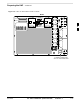
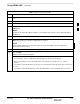
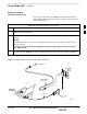
Preparing the LMF – continued Figure 3-6: –48 V SC 4812T Starter Frame I/O Plate REAR SPAN I/O A SITE I/O 1B 2A 2B 3A 3B HSO/ LFR GND 4 2 5 3 6 3 SPAN I/O B FRONT 4A 4B 5A 5B 6A 6B RX LIVE TERMINALS RGD RGPS 1A 1 1 2 3 –48 VDC SPAN I/O A ALARM A LIVE TERMINALS SITE I/O ÄÄÄÄÄÄÄÄÄÄÄÄÄÄÄÄÄÄÄ ÄÄÄÄÄÄÄÄÄÄÄÄÄÄÄÄÄÄÄ ÄÄÄÄÄÄÄÄÄÄÄÄÄÄÄÄÄÄÄ ÄÄÄÄÄÄÄÄÄÄÄÄÄÄÄÄÄÄÄ ÄÄÄÄÄÄÄÄÄÄÄÄÄÄÄÄÄÄÄ ÄÄÄÄÄÄÄÄÄÄÄÄÄÄÄÄÄÄÄ ÄÄÄÄÄÄÄÄÄÄÄÄÄÄÄÄÄÄÄ ÄÄÄÄÄÄÄÄÄÄÄÄÄÄÄÄÄÄÄ ÄÄÄÄÄÄÄÄÄÄÄÄÄÄÄÄÄÄÄ ÄÄÄÄÄÄÄÄÄÄÄÄÄÄÄÄÄÄÄ ÄÄÄÄÄÄ
Using CDMA LMF Basic LMF Operation The CDMA LMF allows the user to work in the two following operating environments, which are accessed using the specified desktop icon: Graphical User Interface (GUI) using the WinLMF icon Command Line Interface (CLI) using the WinLMF CLI icon The GUI is the primary optimization and acceptance testing operating environment.
Using CDMA LMF – continued Command Line Interface Overview The LMF also provides Command Line Interface (CLI) capability. Activate the CLI by clicking on a shortcut icon on the desktop. The CLI can not be launched from the GUI, only from the desktop icon. Both the GUI and the CLI use a program known as the handler. Only one handler can be running at one time Due to architectural limitations, the GUI must be started before the CLI if you want the GUI and CLI to use the same handler.
Using CDMA LMF – continued Logging into a BTS IMPORTANT * 3 Be sure that the correct bts–#.cdf and cbsc–#.cdf file is used for the BTS. These should be the CDF files that are provided for the BTS by the CBSC. Failure to use the correct CDF files can result in invalid optimization. Failure to use the correct CDF files to log into a live (traffic carrying) site can shut down the site. Logging into a BTS establishes a communications link between the BTS and the CDMA LMF.
Using CDMA LMF – continued Table 3-7: BTS GUI Login Procedure Step Action 3 If no base stations are displayed in the Available Base Stations pick list, double click on the CDMA icon. 4 Click on the desired BTS number. 5 Click on the Network Login tab (if not already in the forefront). 6 Enter the correct IP address (normally 128.0.0.2 for a field BTS) if not correctly displayed in the IP Address box. NOTE 128.0.0.2 is the default IP address for MGLI–1 in field BTS units. 128.0.0.
Using CDMA LMF – continued BTS Login from the CLI Environment Follow the procedure in Table 3-8 to log into a BTS when using the CLI environment. IMPORTANT * 3 The GUI and CLI environments use the same connection to a BTS. If a GUI and the CLI session are running for the same BTS at the same time, logging out of the BTS in either environment will log out of it for both. When either a login or logout is performed in the CLI window, there is no GUI indication that logout has occurred.
Using CDMA LMF – continued Table 3-9: BTS GUI Logout Procedure Step Action 1 Click on Select on the BTS tab menu bar. 2 Click the Logout item in the pull–down menu (a Confirm Logout pop–up message appears). 3 Click on Yes or press the key to confirm logout. You are returned to the Login tab. 3 NOTE If a logout was previously performed on the BTS from a CLI window running at the same time as the GUI, a Logout Error pop–up message appears stating the system should not log out of the BTS.
Using CDMA LMF – continued Logging Out of a BTS from the CLI Environment Follow the procedure in Table 3-9 to logout of a BTS when using the CLI environment. Table 3-10: BTS CLI Logout Procedure Step Action * IMPORTANT 3 If the BTS is also logged into from a GUI running at the same time and further work must be done with it in the GUI, proceed to step 2. 1 Logout of a BTS by entering the following command: logout bts– A response similar to the following is displayed: LMF> 12:22:58.
Using CDMA LMF – continued Establishing an MMI Communication Session For those procedures that require MMI communications between the LMF and BTS FRUs, follow the procedure in Table 3-11 to initiate the communication session. Table 3-11: Establishing MMI Communications Step Action 3 1 Connect the LMF computer to the equipment as detailed in the applicable procedure that requires the MMI communication session.
Download the BTS Download the BTS – Overview Before a BTS can operate, each equipped device must contain device initialization (ROM) code. ROM code is loaded in all devices during manufacture or factory repair. Device application (RAM) code and data must be downloaded to each equipped device by the user before the BTS can be made fully functional for the site where it is installed.
Download the BTS – continued Download Code to Devices Code can be downloaded to a device that is in any state. After the download starts, the device being downloaded changes to OOS_ROM (blue). If the download is completed successfully, the device changes to OOS_RAM with code loaded (yellow). Prior to downloading a device, a code file must exist. The code file is selected automatically if the code file is in the /lmf/cdma/n.n.n.n/code folder (where n.n.n.
Download the BTS – continued WARNING R9 RAM code must NOT be downloaded to a device that has R8 ROM code and R8 RAM code must NOT be downloaded to a device that has R9 ROM code. All devices in a BTS must have the same R–level ROM and RAM code before the optimization and ATP procedures can be performed. If a newly installed R8 BTS is to be upgraded to R9, the optimization and ATPs should be accomplished with the R8 code. Then the site should be upgraded to R9 by the CBSC.
Download the BTS – continued Download Code and Data to Non–MGLI2 Devices Non–MGLI2 devices can be downloaded individually or all equipped devices can be downloaded with one action. Follow the procedure in Table 3-13 to download code and data to the non–MGLI2 devices. NOTE When downloading multiple devices, the download may fail for some of the devices (a time out occurs). These devices can be downloaded separately after completing the multiple download.
Download the BTS – continued Follow the procedure in Table 3-14 to select a CSM Clock Source. Table 3-14: Select CSM Clock Source Step 3 Action 1 Select the applicable CSM(s). 2 Click on the Device menu. 3 Click on the Clock Source menu item. 4 Click on the Select menu item. A clock source selection window is displayed. Select the applicable clock source in the Clock Reference Source pick lists. Uncheck the related check box if you do not want the displayed pick list item to be used.
Download the BTS – continued Follow the procedure in Table 3-15 to enable the CSMs. Table 3-15: Enable CSMs Step Action 1 Verify the CSM(s) have been downloaded with code (Yellow, OOS–RAM) and data. 2 Click on the target CSM. From the Device pull down, select Enable. 3 NOTE If equipped with two CSMs, enable CSM–2 first and then CSM–1. A status report confirms change in the device(s) status. Click OK to close the status window. NOTE FAIL may be shown in the status table for enable action.
Download the BTS – continued Enable MCCs This procedure configures the MCC and sets the “tx fine adjust” parameter. The “tx fine adjust” parameter is not a transmit gain setting, but a timing adjustment that compensates for the processing delay in the BTS (approximately 3 ms). Follow the procedure in Table 3-16 to enable the MCCs. IMPORTANT 3 * The MGLI2, and primary CSM must be downloaded and enabled (IN–SERVICE ACTIVE), before downloading and enabling the MCC.
CSM System Time/GPS and LFR/HSO Verification CSM & LFR Background The primary function of the Clock Synchronization Manager (CSM) boards (slots 1 and 2) is to maintain CDMA system time. The CSM in slot 1 is the primary timing source while slot 2 provides redundancy. The CSM2 card (CSM second generation) is required when using the remote GPS receiver (R–GPS). R–GPS uses a GPS receiver in the antenna head that has a digital output to the CSM2 card.
CSM System Time/GPS and LFR/HSO Verification – continued Low Frequency Receiver/ High Stability Oscillator The CSM handles the overall configuration and status monitoring functions of the LFR/HSO. In the event of GPS failure, the LFR/HSO is capable of maintaining synchronization initially established by the GPS reference signal. The LFR requires an active external antenna to receive LORAN RF signals.
CSM System Time/GPS and LFR/HSO Verification – continued Null Modem Cable A null modem cable is required. It is connected between the LMF COM1 port and the RS232–GPIB Interface box. Figure 3-8 shows the wiring detail for the null modem cable.
CSM System Time/GPS and LFR/HSO Verification – continued Table 3-18: Test Equipment Setup (GPS & LFR/HSO Verification) Step Action 3 Reinstall CSM–2. 4 Start an MMI communication session with CSM–1 by using the Windows desktop shortcut icon (see Table 3-5) NOTE The LMF program must not be running when a Hyperterminal session is started if COM1 is being used for the MMI session. 3 When the terminal screen appears, press the key until the CSM> prompt appears.
CSM System Time/GPS and LFR/HSO Verification – continued GPS Initialization/Verification Follow the procedure in Table 3-19 to initialize and verify proper GPS receiver operation. Prerequisites Ensure the following prerequisites have been met before proceeding: The LMF is not logged into the BTS. The COM1 port is connected to the MMI port of the primary CSM via a null modem board (see Figure 3-9). The primary CSM and HSO (if equipped) have been warmed up for at least 15 minutes.
CSM System Time/GPS and LFR/HSO Verification – continued Table 3-19: GPS Initialization/Verification Step Action 3 Verify the following GPS information (underlined text above): – GPS information is usually the 0 reference source. – At least one Primary source must indicate “Status = good” and “Valid = yes” to bring site up. 4 Enter the following command at the CSM> prompt to verify that the GPS receiver is in tracking mode.
CSM System Time/GPS and LFR/HSO Verification – continued Table 3-19: GPS Initialization/Verification Step 6 Action If steps 1 through 5 pass, the GPS is good. * IMPORTANT If any of the above mentioned areas fail, verify that: – If Initial position accuracy is “estimated” (typical), at least 4 satellites must be tracked and visible (1 satellite must be tracked and visible if actual lat, log, and height data for this site has been entered into CDF file).
CSM System Time/GPS and LFR/HSO Verification – continued LFR Initialization/Verification The LORAN–C LFR is a full size card that resides in the C–CCP Shelf. The LFR is a completely self-contained unit that interfaces with the CSM via a serial communications link. The CSM handles the overall configuration and status monitoring functions of the LFR.
CSM System Time/GPS and LFR/HSO Verification – continued Table 3-20: LFR Initialization/Verification Step Action 1 At the CSM> prompt, enter lstatus to verify that the LFR is in tracking mode.
CSM System Time/GPS and LFR/HSO Verification – continued Table 3-20: LFR Initialization/Verification Step Action Note 2 Verify the following LFR information (highlighted above in boldface type): – Locate the “dot” that indicates the current phase locked station assignment (assigned by MM). – Verify that the station call letters are as specified in site documentation as well as M X Y Z assignment. – Verify the signal to noise (S/N) ratio of the phase locked station is greater than 8.
CSM System Time/GPS and LFR/HSO Verification – continued HSO Initialization/Verification The HSO module is a full–size card that resides in the C–CCP Shelf. This completely self contained high stability 10 MHz oscillator interfaces with the CSM via a serial communications link. The CSM handles the overall configuration and status monitoring functions of the HSO.
Test Equipment Set–up Connecting Test Equipment to the BTS All test equipment is controlled by the LMF via an IEEE–488/GPIB bus. The LMF requires each piece of test equipment to have a factory set GPIB address. If there is a communications problem between the LMF and any piece of test equipment, verify that the GPIB addresses have been set correctly (normally 13 for a power meter and 18 for a CDMA analyzer).
Test Equipment Set–up – continued Test Equipment Reference Chart Table 3-22 depicts the current test equipment available meeting Motorola standards. To identify the connection ports, locate the test equipment presently being used in the TEST SETS columns, and read down the column. Where a ball appears in the column, connect one end of the test cable to that port. Follow the horizontal line to locate the end connection(s), reading up the column to identify the appropriate equipment/BTS port.
Test Equipment Set–up – continued Equipment Warm-up IMPORTANT * 3 Warm-up BTS equipment for a minimum of 60 minutes prior to performing the BTS optimization procedure. This assures BTS site stability and contributes to optimization accuracy. (Time spent running initial power-up, hardware/firmware audit, and BTS download counts as warm-up time.) Calibrating Cables Figure 3-10 shows the cable calibration setup for various supported test sets.
Test Equipment Set–up – continued Figure 3-10: Cable Calibration Test Setup SUPPORTED TEST SETS CALIBRATION SET UP Motorola CyberTest A. SHORT CABLE CAL ÏÏÏÏ ÏÏÏÏÌ ANT IN SHORT CABLE TEST SET 3 RF GEN OUT Note: The Directional Coupler is not used with the Cybertest Test Set. The TX cable is connected directly to the Cybertest Test Set. B. RX TEST SETUP A 10dB attenuator must be used with the short test cable for cable calibration with the CyberTest Test Set.
Test Equipment Set–up – continued Setup for TX Calibration Figure 3-11 and Figure 3-12 show the test set connections for TX calibration. Figure 3-11: TX Calibration Test Setup (CyberTest, HP 8935, and Advantest) TEST SETS 3 TRANSMIT (TX) SET UP Motorola CyberTest POWER SENSOR 100–WATT (MIN) NON–RADIATING RF LOAD ÏÏÏ ÏÏÏÌ FRONT PANEL POWER METER (OPTIONAL)* OUT RF IN/OUT 2O DB PAD (FOR 1.7/1.9 GHZ) NOTE: THE DIRECTIONAL COUPLER IS NOT USED WITH THE CYBERTEST TEST SET.
Test Equipment Set–up – continued Figure 3-12: TX Calibration Test Setup HP 8921A W/PCS for 1.7/1.9 GHz TEST SETS TRANSMIT (TX) SET UP Hewlett–Packard Model HP 8921A W/PCS Interface 100–WATT (MIN) NON–RADIATING RF LOAD POWER SENSOR 30 DB DIRECTIONAL COUPLER WITH UNUSED PORT TERMINATED POWER METER 3 TX TEST CABLE 2O DB PAD Note: The HP 8921A cannot be used for TX calibration. A power meter must be used.
Test Equipment Set–up – continued Setup for Optimization/ATP Figure 3-13 and Figure 3-14 show the test set connections for optimization/ATP tests. Figure 3-13: Optimization/ATP Test Setup Calibration (CyberTest, HP 8935 and Advantest) TEST SETS 3 Optimization/ATP SET UP Motorola CyberTest SYNC MONITOR EVEN SEC TICK PULSE REFERENCE FROM CSM BOARD FREQ MONITOR 19.
Test Equipment Set–up – continued Figure 3-14: Optimization/ATP Test Setup HP 8921A TEST SETS Optimization/ATP SET UP Hewlett–Packard Model HP 8921A W/PCS Interface (for 1700 and 1900 MHz) SYNC MONITOR EVEN SEC TICK PULSE REFERENCE FROM CSM BOARD FREQ MONITOR 19.6608 MHZ CLOCK REFERENCE FROM CSM BOARD NOTE: IF BTS RX/TX SIGNALS ARE DUPLEXED (4800E): BOTH THE TX AND RX TEST CABLES CONNECT TO THE DUPLEXED ANTENNA GROUP.
Test Equipment Set–up – continued Figure 3-15: Typical TX ATP Setup with Directional Coupler (shown with and without RFDS) TX ANTENNA DIRECTIONAL COUPLERS COBRA RFDS Detail RX (RFM TX) TX RF FROM BTS FRAME 3 TX (RFM RX) 2 1 RFDS RX (RFM TX) COUPLER OUTPUTS TO RFDS FWD(BTS) ASU2 (SHADED) CONNECTORS 3 RF FEED LINE TO DIRECTIONAL COUPLER REMOVED Connect TX test cable between the directional coupler input port and the appropriate TX antenna directional coupler connector.
Test Equipment Set–up – continued Figure 3-16: Typical RX ATP Setup with Directional Coupler (shown with or without RFDS) COBRA RFDS Detail RX ANTENNA DIRECTIONAL COUPLERS RX RF FROM BTS FRAME 2 3 4 5 6 RX (RFM TX) 1 TX (RFM RX) RFDS TX (RFM RX) COUPLER OUTPUTS TO RFDS FWD(BTS) ASU1 (SHADED) CONNECTORS 3 RF FEED LINE TO TX ANTENNA REMOVED Connect RX test cable between the test set and the appropriate RX antenna directional coupler.
Test Set Calibration Test Set Calibration Background Proper test equipment calibration ensures that the test equipment and associated test cables do not introduce measurement errors, and that measurements are correct. NOTE 3 If the test set being used to interface with the BTS has been calibrated and maintained as a set, this procedure does not need to be performed. (Test Set includes LMF terminal, communications test set, additional test equipment, associated test cables, and adapters.
Test Set Calibration – continued Selecting Test Equipment Use LMF Options from the Options menu list to select test equipment automatically (using the autodetect feature) or manually. A Serial Connection and a Network Connection tab are provided for test equipment selection. The Serial Connection tab is used when the test equipment items are connected directly to the LMF computer via a GPIB box (normal setup).
Test Set Calibration – continued Automatically Selecting Test Equipment in a Serial Connection Tab When using the auto-detection feature to select test equipment, the LMF examines which test equipment items are actually communicating with the LMF. Follow the procedure in Table 3-24 to use the auto-detect feature. Table 3-24: Selecting Test Equipment Using Auto-Detect 3 Step Action 1 From the Options menu, select LMF Options. The LMF Options window appears.
Test Set Calibration – continued Calibrating Test Equipment The calibrate test equipment function zeros the power measurement level of the test equipment item that is to be used for TX calibration and audit. If both a power meter and an analyzer are connected, only the power meter is zeroed. Use the Calibrate Test Equipment menu item from the Util menu to calibrate test equipment. The test equipment must be selected before calibration can begin.
Test Set Calibration – continued The short cable plus the TX cable configuration loss is measured – The TX cable configuration normally consists of two coax cables with type-N connectors and a directional coupler, a load, and an additional attenuator (if required by the specified BTS). The total loss of the path loss of the TX cable configuration must be as required for the BTS (normally 30 or 50 dB).
Test Set Calibration – continued Calibrating TX Cables Using a Signal Generator and Spectrum Analyzer Follow the procedure in Table 3-27 to calibrate the TX cables using a signal generator and spectrum analyzer. Refer to Figure 3-17 for a diagram of the signal generator and spectrum analyzer. Table 3-27: Calibrating TX Cables Using Signal Generator and Spectrum Analyzer Step Action 3 1 Connect a short test cable between the spectrum analyzer and the signal generator.
Test Set Calibration – continued Figure 3-17: Calibrating Test Equipment Setup for TX BLO and TX ATP Tests (using Signal Generator and Spectrum Analyzer) Signal Generator Spectrum Analyzer SHORT TEST CABLE 3 40W NON–RADIATING RF LOAD THIS WILL BE THE CONNECTION TO THE TX PORTS DURING TX BAY LEVEL OFFSET TEST AND TX ATP TESTS.
Test Set Calibration – continued Table 3-28: Calibrating RX Cables Using a Signal Generator and Spectrum Analyzer Step 5 Action Calibration factor = A – B Example: Cal = –12 dBm – (–14 dBm) = 2 dBm NOTE The short test cable is used for test equipment setup calibration only. It is not be part of the final test setup. After calibration is completed, do not re-arrange any cables. Use the equipment setup, as is, to ensure test procedures use the correct calibration factor.
Test Set Calibration – continued Setting Cable Loss Values Cable loss values for the TX and RX test cable configurations are normally set by accomplishing cable calibration using the applicable test equipment. The resulting values are stored in the cable loss files. The cable loss values can also be set/changed manually. Follow the procedure in Table 3-29 to set cable loss values. Prerequisites Logged into the BTS 3 Table 3-29: Setting Cable Loss Values Step Action 1 Click on the Util menu.
Test Set Calibration – continued Setting TX Coupler Loss Value If an in–service TX coupler is installed, the coupler loss (e.g., 30 dB) must be manually entered so it will be included in the LMF TX calibration and audit calculations. Follow the procedure in Table 3-30 to set TX coupler loss values. Prerequisites Logged into the BTS. 3 Table 3-30: Setting TX Coupler Loss Value Step Action 1 Click on the Util menu. 2 Select Edit>TX Coupler Loss. A data entry pop–up window appears.
Bay Level Offset Calibration Introduction to Bay Level Offset Calibration Calibration compensates for normal equipment variations within the BTS and assures maximum measurement accuracy. RF Path Bay Level Offset Calibration 3 Calibration identifies the accumulated gain in every transmit path (BBX slot) at the BTS site and stores that value in a BLO database calibration table in the LMF. The BLOs are subsequently downloaded to each BBX.
Bay Level Offset Calibration – continued – TX filter / TX filter combiner – TX thru-port cable to the top of frame TX Path Calibration The TX Path Calibration assures correct site installation, cabling, and the first order functionality of all installed equipment. The proper function of each RF path is verified during calibration. The external test equipment is used to validate/calibrate the TX paths of the BTS.
Bay Level Offset Calibration – continued BLO Calibration Data File During the calibration process, the LMF creates a bts–n.cal calibration (BLO) offset data file in the bts–n folder. After calibration has been completed, this offset data must be downloaded to the BBXs using the Download BLO function. An explanation of the file is shown below. NOTE 3 Due to the size of the file, Motorola recommends that you print out a hard copy of a bts.cal file and refer to it for the following descriptions.
Bay Level Offset Calibration – continued – The second breakdown of the array is per sector. Configurations supported are Omni, 3–sector or 6–sector. Table 3-32: BTS.
Bay Level Offset Calibration – continued The 20 calibration entries for each sector/branch combination must be stored in order of increasing frequency. If less than 10 points (frequencies) are calibrated, the largest frequency that is calibrated is repeated to fill out the 10 points. Example: C[1]=384, odd cal entry = 1 ‘‘calibration point” C[2]=19102, even cal entry C[3]=777, C[4]=19086, . .
Bay Level Offset Calibration – continued TX Path Calibration The assigned channel frequency and power level (as measured at the top of the frame) for transmit calibration are derived from the site CDF files. For each BBX, the channel frequency is specified in the ChannelList CDF file parameter and the power is specified in the SIFPilotPwr CDF file parameter for the sector associated with the BBX (located under the ParentSECTOR field of the ParentCARRIER CDF file parameter). 3 NOTE If both the BTS–x.
Bay Level Offset Calibration – continued Connect the test equipment as shown in Figure 3-11 and Figure 3-12 and follow the procedure in Table 3-34 to perform the TX calibration test. WARNING Before installing any test equipment directly to any TX OUT connector, first verify there are no CDMA BBX channels keyed. Failure to do so can result in serious personal injury and/or equipment damage. 3 IMPORTANT * Verify all BBX boards removed and repositioned have been returned to their assigned shelves/slots.
Bay Level Offset Calibration – continued Download BLO Procedure After a successful TX path calibration, download the bay level offset (BLO) calibration file data to the BBXs. BLO data is extracted from the CAL file for the Base Transceiver Subsystem (BTS) and downloaded to the selected BBX devices. NOTE If a successful All Cal/Audit was completed, this procedure does not need to be performed, as BLO is downloaded as part of the All Cal/Audit.
Bay Level Offset Calibration – continued TX Path Audit Perform the calibration audit of the TX paths of all equipped BBX slots, per the procedure in Table 3-36 WARNING Before installing any test equipment directly to any TX OUT connector, first verify there are no CDMA BBX channels keyed. Failure to do so can result in serious personal injury and/or equipment damage.
Bay Level Offset Calibration – continued Table 3-36: BTS TX Path Audit Step Action 1 Select the BBX(s) to be audited. 2 From the Tests menu, select TX Audit. 3 4 Select the appropriate carrier(s) displayed in the Channels/Carrier pick list. Press and hold the or key to select multiple items. Type the appropriate channel number in the Carrier n Channels box. 5 Click on OK. 6 Follow the cable connection directions as they are displayed.
Bay Level Offset Calibration – continued Prerequisites Before running this test, ensure that the following have been done: 3 CSM–1, GLI2s, BBXs have correct code and data loads. Primary CSM and MGLI2 are INS. All BBXs are OOS_RAM. Test equipment and test cables are calibrated and connected for TX BLO calibration. LMF is logged into the BTS. Follow the procedure in Table 3-37 to perform the All Cal/Audit test.
Bay Level Offset Calibration – continued Create CAL File The Create Cal File function gets the BLO data from BBXs and creates/updates the CAL file for the BTS. If a CAL file does not exist, a new one is created. If a CAL file already exists, it is updated. After a BTS has been fully optimized, a copy of the CAL file must exist so it can be transferred to the CBSC. If TX calibration has been successfully performed for all BBXs and BLO data has been downloaded, a CAL file exists.
RFDS Setup and Calibration RFDS Description NOTE The RFDS is not available for the –48 V BTS at the time of this publication. 3 The optional RFDS performs RF tests of the site from the CBSC or from an LMF. The RFDS consists of the following elements: Antenna Select Unit (ASU) FWT Interface Card (FWTIC) Subscriber Unit Assembly (SUA) For complete information regarding the RFDS, refer to the CDMA RFDS Hardware Installation manual and CDMA RFDS User’s Guide.
RFDS Setup and Calibration – continued RFDS Parameter Settings The bts-#.cdf file includes RFDS parameter settings that must match the installed RFDS equipment. The paragraphs below describe the editable parameters and their defaults. Table 3-39 explains how to edit the parameter settings. RfdsEquip – valid inputs are 0 through 2.
RFDS Setup and Calibration – continued Table 3-39: RFDS Parameter Settings Step Action * IMPORTANT Log out of the BTS prior to performing this procedure. 1 3 Using a text editor, verify the following fields are set correctly in the bts–#.cdf file (1 = GLI based RFDS; 2 = Cobra RFDS). EXAMPLE: RfdsEquip = 2 TsuEquip = 1 MC1Equip = 0 MC2Equip = 0 MC3Equip = 0 MC4Equip = 0 Asu1Equip = 1 Asu2Equip = 0 (1 if system is non-duplexed) TestOrigDN = ’123456789’’ NOTE The above is an example of the bts-#.
RFDS Setup and Calibration – continued RFDS TSU NAM Programming The RFDS TSU NAM must be programmed with the appropriate system parameters and phone number during hardware installation. The TSU phone and TSU MSI must be recorded for each BTS used for OMC–R RFDS software configuration. The TSU NAM should be configured the same way that any local mobile subscriber would use. NOTE The user will only need to program the NAM for the initial install of the RFDS.
RFDS Setup and Calibration – continued Valid NAM Ranges Table 3-41 provides the valid NAM field ranges. If any of the fields are missing or out of range, the RFDS errors out.
RFDS Setup and Calibration – continued Set Antenna Map Data The antenna map data is only used for RFDS tests and is required if an RFDS is installed. Antenna map data does not have to be entered if an RFDS is not installed. The antenna map data must be entered manually. Perform the procedure in Table 3-42 to set the Antenna Map Data. Prerequisite Logged into the BTS 3 Table 3-42: Set Antenna Map Data Step Action 1 Click on the Util menu. 2 Select Edit>Antenna Map>TX or RX.
RFDS Setup and Calibration – continued Set RFDS Configuration Data If an RFDS is installed, the RFDS configuration data must be manually entered. Perform the procedure in Table 3-43 to set the RFDS Configuration Data. Prerequisite Logged into the BTS. 3 IMPORTANT * The entered antenna# index numbers must correspond to the antenna# index numbers used in the antenna maps. Table 3-43: Set RFDS Configuration Data Step Action 1 Click on the Util menu. 2 Select Edit>RFDS Configuration>TX or RX.
RFDS Setup and Calibration – continued RFDS Calibration The RFDS TX and RX antenna paths must be calibrated to ensure peak performance. The RFDS calibration option calibrates the RFDS TX and RX paths. For a TX antenna path calibration, the BTS XCVR is keyed at a pre–determined power level and the BTS power output level is measured by the RFDS. The power level is then measured at the TX antenna directional coupler by the power measuring test equipment item being used (power meter or analyzer).
RFDS Setup and Calibration – continued Table 3-44: RFDS Calibration Procedure Step 6 Action Select the appropriate carrier(s) in the Carriers pick list. NOTE Use the or key to select multiple carriers. 3 7 Select the appropriate Rx branch (Main, Diversity or Both) in the RX Branch pick list. 8 Select the appropriate baud rate (1=9600, 2=14400) in the Rate Set pick list. 9 Click OK. A status report window is displayed, followed by a Directions pop-up window.
BTS Redundancy/Alarm Testing Objective This section tests the redundancy options that could be included in the cell site. These tests verify, under a fault condition, that all modules equipped with redundancy switch operations to their redundant partner and resume operation. An example would be to pull the currently active CSM and verify the standby CSM takes over distribution of the CDMA reference signal. Redundancy covers many BTS modules.
BTS Redundancy/Alarm Testing – continued Test Equipment Setup Follow the procedure in Table 3-46 to set up test equipment: NOTE All alarm tests are performed using TX antenna 1 Table 3-46: Test Equipment Setup for Redundancy/Alarm Tests 3 Step Action 1 Interface the LMF computer to the BTS LAN A connector on the BTS frame (refer to Table 3-2, page 3-5). 2 Login to the BTS. 3 Set up test equipment for TX Calibration at TXOUT1 (see Figure 3-11 or Figure 3-12).
BTS Redundancy/Alarm Testing – continued Power Supply Redundancy Follow the steps in Table 3-47 to verify redundancy of the power supply modules. Alarms reported by the master GLI (displayed via the alarm monitor) are also verified.
3-88 CCD–1 CCD–2 PS–2 CSM–2 PS–6 GLI2–2 GLI2–1 MCC24–7 MCC24–1 MCC24–8 MCC24–2 MCC24–9 MCC24–3 MCC24–10 MCC24–4 MCC24–11 MCC24–5 MCC24–12 MCC24–6 BBX2–7 BBX2–1 BBX2–8 BBX2–2 BBX2–9 BBX2–3 BBX2–10 BBX2–4 BBX2–11 BBX2–5 FAN MODULE PWR/ALM 1B 3B 2D 1A 30 30 2B 30 4B 3D 4D 3C 30 4C 30 4A 30 L 2C P A 3A 1D CIO 2A 30 BBX2–R 1C 30 BBX2–6 Switch 68P09253A61 SCt4812T CDMA BTS Optimization/ATP PS–9 REAR FRONT PS–8 AMR–1 AMR–2 MPC/EMPC–1 MPC/EMPC–2 PS–3 38 mm Filler Panel PS
BTS Redundancy/Alarm Testing – continued Miscellaneous Alarm/Redundancy Tests Follow the steps in Table 3-48 to verify alarms reported by the master GLI are displayed via the alarm monitor if a BTS frame module failure occurs. Table 3-48: Miscellaneous Alarm Tests Step Action 1 Select Util>Alarm Monitor to display the alarm monitor window. 2 Perform the following to verify fan module alarms: • Unseat a fan module (see Figure 3-21 or Figure 3-22).
BTS Redundancy/Alarm Testing – continued Figure 3-21: +27 V BTS C-CCP Fan Modules LATCHES FAN MODULE REAR FAN MODULE REAR REAR PWR/ALM FRONT 3 FAN MODULE PWR/ALM FRONT PWR/ALM FRONT FAN MODULES FW00130 Figure 3-22: –48 V BTS C-CCP and Power Conversion Shelf Fan Modules LATCHES FAN MODULE REAR FRONT FAN MODULE REAR PWR/ALM FRONT FAN MODULE REAR PWR/ALM FRONT PWR/ALM FAN MODULES LATCHES FAN MODULE REAR FRONT FAN MODULE REAR PWR/ALM FRONT PWR/ALM FW00489 FAN MODULES 3-90 SCt48
BTS Redundancy/Alarm Testing – continued BBX Redundancy Follow the steps in Table 3-49 to verify redundancy of the BBXs in the C–CCP shelf. Alarms reported by the master GLI (displayed via the alarm monitor) are also verified. This test can be repeated for additional sectors at the customer’s discretion. Table 3-49: BBX Redundancy Alarms Step Action 3 n WARNING Any BBXs enabled will immediately key-up.
BTS Redundancy/Alarm Testing – continued CSM, GPS, & LFR/HSO Redundancy/Alarm Tests Follow the procedure in Table 3-50 to verify the manual redundancy of the CSM, GPS, and LFR/HSO boards. Verification of alarms reported is also covered. IMPORTANT * 3 DO NOT perform the procedure in Table 3-50, unless the site is configured with a LORAN–C or HSO timebase as a backup for the GPS. Table 3-50: CSM, GPS, & LFR/HSO, Redundancy/Alarm Tests Step Action n WARNING Any BBXs enabled will immediately key-up.
BTS Redundancy/Alarm Testing – continued Table 3-50: CSM, GPS, & LFR/HSO, Redundancy/Alarm Tests Step 8 Action Allow the CSM 2 board to go INS_ACT. Verify the BBXs are dekeyed and OOS, and the MCCs are OOS_RAM. Verify no other modules went OOS due to the transfer to CSM 2 reference. Observe the PWR/ALM LEDs on CSM 2 front panels are steady GREEN. 3 NOTE It can take up to 20 minutes for the CSM to re-establish the GPS link and go INS. MCCs go OOS_RAM.
BTS Redundancy/Alarm Testing – continued Figure 3-23: +27 V SC 4812T Starter Frame I/O Plate REAR SPAN I/O A RGPS SPAN I/O A SITE I/O 1B 2A SPAN I/O B LFR/ HSO 2 5 3 6 2B GND RX 3A 3B 4A 4B 5A 5B 6A 6B LIVE TERMINALS RGD 3 1A +27 VDC ALARM A 4 LIVE TERMINALS ÄÄÄÄÄÄÄÄÄÄÄÄÄÄÄÄÄÄÄ ÄÄÄÄÄÄÄÄÄÄÄÄÄÄÄÄÄÄÄ ÄÄÄÄÄÄÄÄÄÄÄÄÄÄÄÄÄÄÄ ÄÄÄÄÄÄÄÄÄÄÄÄÄÄÄÄÄÄÄ ÄÄÄÄÄÄÄÄÄÄÄÄÄÄÄÄÄÄÄ ÄÄÄÄÄÄÄÄÄÄÄÄÄÄÄÄÄÄÄ ÄÄÄÄÄÄÄÄÄÄÄÄÄÄÄÄÄÄÄ ÄÄÄÄÄÄÄÄÄÄÄÄÄÄÄÄÄÄÄ ÄÄÄÄÄÄÄÄÄÄÄÄÄÄÄÄÄÄÄ ÄÄÄÄÄÄÄÄÄÄÄÄÄÄÄÄÄÄÄ ÄÄÄÄÄÄÄÄÄÄÄÄÄÄÄÄÄÄÄ ÄÄÄÄ
BTS Redundancy/Alarm Testing – continued LPA Redundancy Test Follow the procedure in Table 3-51 to verify redundancy of the LPAs. WARNING First verify there are no BBX channels keyed BEFORE moving the antenna connection. Failure to do so can result in serious personal injury and/or equipment damage.
BTS Redundancy/Alarm Testing – continued MGLI/GLI Redundancy Test CAUTION This test can only be performed when the MM path is established by the MM (not just with LAPD link connected). Attempting to force the GLIs to “hot swap” under alarm monitor control, when isolated from the MM, causes MGLIs to hang up.
BTS Alarms Testing Alarm Test Overview ALARM connectors provide Customer Defined Alarm Inputs and Outputs. The customer can connect BTS site alarm input sensors and output devices to the BTS, thus providing alarm reporting of active sensors as well controlling output devices. The SC 4812T is capable of concurrently monitoring 36 input signals coming into the BTS. These inputs are divided between 2 Alarm connectors marked ‘ALARM A’ and ‘ALARM B’ located at the top of the frame (see Figure 3-24).
BTS Alarms Testing – continued Figure 3-24: Alarm Connector Location and Connector Pin Numbering ÂÂÂÂÂÂ ÂÂÂÂÂÂ ÂÂÂÂÂÂ ÂÂÂÂÂÂ ÂÂÂÂÂÂ Á ÁÁ Á Á 3 1 1 2 2 59 59 60 60 FW00301 Purpose The following procedures verify the customer defined alarms and relay contacts are functioning properly. These tests are performed on all AMR alarms/relays in a sequential manner until all have been verified. Perform these procedures periodically to ensure the external alarms are reported properly.
BTS Alarms Testing – continued NOTE Abbreviations used in the following figures and tables are defined as: NC = normally closed NO = normally open COM or C = common CDO = Customer Defined (Relay) Output CDI = Customer Defined (Alarm) Input 3 Figure 3-25: AMR Connector Pin Numbering A CDI 18 ... A CDI 1 Returns 60 26 2 60 26 59 25 1 59 25 ALARM A (AMR 1) Returns 2 1 ALARM B (AMR 2) B CDI 36 ...
BTS Alarms Testing – continued Table 3-53: CDI Alarm Input Verification Using the Alarms Test Box Step 3 Action 3 Click on the Device menu. 4 Click on the Customer Alarm Inputs menu item. 5 Click on N.O. Inputs. A status report window displays the results of the action. 6 Click on the OK button to close the status report window. 7 Set all switches on the alarms test box to the Open position. 8 Connect the alarms test box to the ALARM A connector (see Figure 3-24).
BTS Alarms Testing – continued Table 3-53: CDI Alarm Input Verification Using the Alarms Test Box Step Action 26 Connect the alarms test box to the ALARM B connector. A clear alarm should be reported for alarm inputs 19 through 36. 27 Set all switches on the alarms test box to the Open position. An alarm should be reported for each switch setting. 28 Set all switches on the alarms test box to the Closed position. A clear alarm should be reported for each switch setting.
BTS Alarms Testing – continued CDI Alarm Input Verification without Alarms Test Box Table 3-54 describes how to test the CDI alarm input verification without the use of the Alarms Test Box. Follow the steps as instructed and compare results with the LMF display. NOTE 3 It may take a few seconds for alarms to be reported. The default delay is 5 seconds. When shorting alarm pins wait for the alarm report before removing the short.
BTS Alarms Testing – continued Table 3-54: CDI Alarm Input Verification Without the Alarms Test Box Step Action 14 Refer to Figure 3-25 and sequentially short the ALARM A connector CDI 1 through CDI 18 pins (25–26 through 59–60) together. A clear alarm should be reported for each pair of pins that are shorted. An alarm should be reported for each pair of pins when the short is removed.
BTS Alarms Testing – continued Table 3-55: Pin and Signal Information for Alarm Connectors ALARM A Pin 3 Signal Name ALARM B Pin Signal Name Pin Signal Name Pin Signal Name 7 A CDO3 NC 37 Cust Retn 7 7 B CDO11 NC 37 B CDI 25 8 A CDO3 Com 38 A CDI 7 8 B CDO11 Com 38 Cust Retn 25 9 A CDO3 NO 39 Cust Retn 8 9 B CDO11 NO 39 B CDI 26 10 A CDO4 NC 40 A CDI 8 10 B CDO12 NC 40 Cust Retn 26 11 A CDO4 Com 41 Cust Retn 9 11 B CDO12 Com 41 B CDI 27 12 A CDO4 NO 42 A
Chapter 4: Automated Acceptance Test Procedure (ATP) Table of Contents Mar 2001 Automated Acceptance Test Procedures – All–inclusive TX & RX . . . . . . . . . Introduction . . . . . . . . . . . . . . . . . . . . . . . . . . . . . . . . . . . . . . . . . . . . . . ATP Test Prerequisites . . . . . . . . . . . . . . . . . . . . . . . . . . . . . . . . . . . . . . TX OUT Connection . . . . . . . . . . . . . . . . . . . . . . . . . . . . . . . . . . . . . . . ATP Test Procedure . . . . . . . . . . . . . . . .
Table of Contents – continued Notes 4 SCt4812T CDMA BTS Optimization/ATP Mar 2001 DRAFT
Automated Acceptance Test Procedures – All–inclusive TX & RX Introduction The Automated Acceptance Test Procedure (ATP) allows Cellular Field Engineers (CFEs) to run automated acceptance tests on all equipped BTS subsystem devices using the Local Maintenance Facility (LMF) and supported test equipment per the current Cell Site Data File (CDF) assignment. The results of these tests (at the option of the operator) are written to a file that can be printed.
Automated Acceptance Test Procedure – All–inclusive TX & RX – continued All TX/RX: Executes all the TX and RX tests. Full Optimization: Executes the TX calibration, downloads the BLO, and executes the TX audit before running all of the TX and RX tests. ATP Test Prerequisites Before attempting to run any ATP tests, ensure the following have been completed: BTS has been optimized and calibrated (see Chapter 3). LMF is logged into the BTS.
Automated Acceptance Test Procedure – All–inclusive TX & RX – continued ATP Test Procedure There are three different ATP testing options that can be performed to completely test a BTS. Depending on your requirements, one of the following ATP testing options should be run.
Automated Acceptance Test Procedure – All–inclusive TX & RX – continued Table 4-1: ATP Test Procedure Step Action 4 Enter the appropriate channel number in the Carrier n Channels box. The default channel number displayed is determined by the CdmaChans[n] number in the cbsc–n.cdf file for the BTS. 5 Click on the OK button. The status report window and a Directions pop-up are displayed. Follow the cable connection directions as they are displayed.
TX Output Acceptance Tests: Introduction Individual Acceptance Tests The following individual tests can be used to verify the results of specific tests. Spectral Purity TX Mask (Primary & Redundant BBX) This test verifies that the transmitted CDMA carrier waveform generated on each sector meets the transmit spectral mask specification with respect to the assigned CDF file values.
TX Spectral Purity Transmit Mask Acceptance Test Tx Mask Test This test verifies the spectral purity of each BBX carrier keyed up at a specific frequency, per the current CDF file assignment. All tests are performed using the external calibrated test set, controlled by the same command. All measurements are via the appropriate TX OUT (BTS/RFDS) connector. The Pilot Gain is set to 541 for each antenna, and all channel elements from the MCCs are forward-link disabled.
TX Spectral Purity Transmit Mask Acceptance Test – continued Figure 4-1: TX Mask Verification Spectrum Analyzer Display Mean CDMA Bandwidth Power Reference .
TX Waveform Quality (rho) Acceptance Test Rho Test This test verifies the transmitted Pilot channel element digital waveform quality of each BBX carrier keyed up at a specific frequency per the current CDF file assignment. All tests are performed using the external calibrated test set controlled by the same command. All measurements are via the appropriate TX OUT (BTS/RFDS) connector. The Pilot Gain is set to 262 for each antenna, and all channel elements from the MCCs are forward link disabled.
TX Pilot Time Offset Acceptance Test Pilot Offset Acceptance Test This test verifies the transmitted Pilot channel element Pilot Time Offset of each BBX carrier keyed up at a specific frequency per the current CDF file assignment. All tests are performed using the external calibrated test set controlled by the same command. All measurements are via the appropriate TX OUT (BTS/RFDS) connector. The Pilot Gain is set to 262 for each antenna, and all TCH elements from the MCCs are forward link disabled.
TX Code Domain Power/Noise Floor Acceptance Test Code Domain Power Test This test verifies the Code Domain Power/Noise of each BBX carrier keyed up at a specific frequency per the current CDF file assignment. All tests are performed using the external calibrated test set controlled by the same command. All measurements are via the appropriate TX OUT (BTS/RFDS) connector. For each sector/antenna under test, the Pilot Gain is set to 262.
TX Code Domain Power/Noise Floor Acceptance Test – continued Figure 4-2: Code Domain Power and Noise Floor Levels Pilot Channel PILOT LEVEL MAX OCNS CHANNEL 8.2 dB 12.2 dB MAX OCNS SPEC. Active channels MIN OCNS SPEC. MIN OCNS CHANNEL MAX NOISE FLOOR MAXIMUM NOISE FLOOR: < –27 dB SPEC. 4 Inactive channels Walsh 0 1 2 3 4 5 6 7 ... 64 Showing all OCNS Passing Pilot Channel PILOT LEVEL FAILURE – EXCEEDS MAX OCNS SPEC. 8.2 dB 12.2 dB MAX OCNS SPEC. Active channels MIN OCNS SPEC.
RX Frame Error Rate (FER) Acceptance Test FER Test This test verifies the BTS FER on all traffic channel elements currently configured on all equipped MCCs (full rate at 1% FER) at an RF input level of –119 dBm [or –116 dBm if using Tower Top Amplifier (TMPC)]. All tests are performed using the external calibrated test set as the signal source controlled by the same command. All measurements are via the LMF.
Generate an ATP Report Background Each time an ATP test is run, an ATP report is updated to include the results of the most recent ATP tests if the Save Results button is used to close the status report window. The ATP report is not updated if the status reports window is closed using the Dismiss button.
Generate an ATP Report – continued Notes 4 4-14 SCt4812T CDMA BTS Optimization/ATP Mar 2001 DRAFT
Chapter 5: Prepare to Leave the Site Table of Contents Prepare to Leave the Site . . . . . . . . . . . . . . . . . . . . . . . . . . . . . . . . . . . . . . . . . . External Test Equipment Removal . . . . . . . . . . . . . . . . . . . . . . . . . . . . Reset All Devices . . . . . . . . . . . . . . . . . . . . . . . . . . . . . . . . . . . . . . . . . BTS Site Span Configuration Verification . . . . . . . . . . . . . . . . . . . . . . Set BTS Site Span Configuration . . . . . . . . . . . . . . . . . . . . .
Table of Contents – continued Notes 5 SCt4812T CDMA BTS Optimization/ATP Mar 2001 DRAFT
Prepare to Leave the Site External Test Equipment Removal Perform the procedure in Table 5-1 to disconnect the test equipment and configure the BTS for active service. Table 5-1: External Test Equipment Removal Step Action 1 Disconnect all external test equipment from all TX and RX connectors on the top of the frame. 2 Reconnect and visually inspect all TX and RX antenna feed lines at the top of the frame.
Prepare to Leave the Site – continued Reset All Devices Reset all devices by cycling power before leaving the site. The configuration data and code loads could be different from data and code on the LMF. By resetting all devices, the CBSC can load the proper data and code when the span is active again. Follow the procedure in Table 5-2 as required to bring all processor modules from the OOS to INS mode. IMPORTANT * Have the CBSC/MM bring up the site and enable all devices at the BTS.
Prepare to Leave the Site – continued Re–connect BTS T1 Spans and Integrated Frame Modem Before leaving the site, connect any T1 span TELCO connectors that were removed to allow the LMF to control the BTS. Refer to Table 5-3 and Figure 5-1 as required. Table 5-3: T1/E1 Span/IFM Connections Step Action 1 Connect the 50–pin TELCO cables to the BTS span I/O board 50–pin TELCO connectors. 2 If used, connect the dial–up modem RS–232 serial cable to the Site I/O board RS–232 9–pin sub D connector.
Prepare to Leave the Site – continued BTS Site Span Configuration Verification Perform the procedure in Table 5-4 to verify the current Span Framing Format and Line Build Out (LBO) parameters. ALL MGLI2/SGLI2 boards in all C–CCP shelves that terminate a T1/E1 span should be verified. Table 5-4: BTS Span Parameter Configuration Step Action 1 Connect a serial cable from the LMF COM1 port (via null modem board) to the front panel of the MGLI2 MMI port (see Figure 5-2).
Prepare to Leave the Site – continued Table 5-4: BTS Span Parameter Configuration Step Action 4 Repeat steps 1 through 3 for all remaining GLIs. 5 Exit the GLI MMI session and HyperTerminal connection by selecting File from the connection window menu bar, and then Exit from the dropdown menu.
Prepare to Leave the Site – continued Table 5-5: Set BTS Span Parameter Configuration Step Action 1 If not already done, connect a serial cable from the LMF COM1 port (via null modem board) to the front panel of the MGLI2 MMI port (see Figure 5-2). 2 Start an MMI communication session with CSM–1 by using the Windows desktop shortcut icon (see Table 3-5 on page 3-11).
Prepare to Leave the Site – continued Table 5-5: Set BTS Span Parameter Configuration Step Action * IMPORTANT Make sure that spans a – f are set to the same span type and link speed. The equalization may be different for each individual span. After executing the span_config command, the affected MGLI2/SGLI2 board MUST be reset and re–loaded for changes to take effect. Although defaults are shown, always consult site specific documentation for span type and rate used at the site.
Prepare to Leave the Site – continued LMF Removal CAUTION DO NOT power down the LMF without performing the procedure indicated below. Corrupted/lost data files may result, and in some cases, the LMF may lock up. Follow the procedure in Table 5-7 to terminate the LMF session and remove the terminal. Table 5-7: LMF Termination and Removal Step 5 Action 1 From the CDMA window select File>Exit. 2 From the Windows Task Bar click Start>Shutdown. Click Yes when the Shut Down Windows message appears.
Prepare to Leave the Site – continued Table 5-8: Procedures to Copy CAL Files from Diskette to the CBSC Step Action 8 Enter pwd and press the key. Verify that you are in your home directory (/home/). 9 Enter dos2unix /floppy/no_name/bts–#.cal bts–#.cal and press the key (where # is the BTS number). 10 Enter ls –l *.cal and press the key. Verify that the CAL file was successfully copied. 11 Type eject and press the key.
Prepare to Leave the Site – continued Notes 5 5-10 SCt4812T CDMA BTS Optimization/ATP Mar 2001 DRAFT
Chapter 6: Basic Troubleshooting Table of Contents Mar 2001 Basic Troubleshooting Overview . . . . . . . . . . . . . . . . . . . . . . . . . . . . . . . . . . . . Overview . . . . . . . . . . . . . . . . . . . . . . . . . . . . . . . . . . . . . . . . . . . . . . . . 6-1 6-1 Troubleshooting: Installation . . . . . . . . . . . . . . . . . . . . . . . . . . . . . . . . . . . . . . . Cannot Log into Cell-Site . . . . . . . . . . . . . . . . . . . . . . . . . . . . . . . . . . .
Table of Contents – continued DC Power Problems . . . . . . . . . . . . . . . . . . . . . . . . . . . . . . . . . . . . . . . TX and RX Signal Routing Problems . . . . . . . . . . . . . . . . . . . . . . . . . . 6-18 6-19 Module Front Panel LED Indicators and Connectors . . . . . . . . . . . . . . . . . . . . . Module Status Indicators . . . . . . . . . . . . . . . . . . . . . . . . . . . . . . . . . . . . LED Status Combinations for All Modules (except GLI2, CSM, BBX2, MCC24, MCC8E) . . . . . . . . . .
Basic Troubleshooting Overview Overview The information in this section addresses some of the scenarios likely to be encountered by Cellular Field Engineering (CFE) team members. This troubleshooting guide was created as an interim reference document for use in the field. It provides basic “what to do if” basic troubleshooting suggestions when the BTS equipment does not perform per the procedure documented in the manual.
Troubleshooting: Installation Cannot Log into Cell-Site Follow the procedure in Table 6-1 to troubleshoot a login failure. Table 6-1: Login Failure Troubleshooting Procedures Step Action 1 If MGLI2 LED is solid RED, it implies a hardware failure. Reset MGLI2 by re-seating it. If this persists, install a known good MGLI2 card in MGLI2 slot and retry. A Red LED may also indicate no Ethernet termination at top of frame. 2 Verify that T1 is disconnected (see Table 3-1 on page 3-4).
Troubleshooting: Installation – continued Table 6-2: Troubleshooting a Power Meter Communication Failure Step Action 5 Verify the GPIB adapter is not locked up. Under normal conditions, only two green LEDs must be ‘ON’ (Power and Ready). If any other LED is continuously ‘ON’, then power-cycle the GPIB Box and retry. 6 Verify that the Com1 port is not used by another application. 7 Verify that the communications analyzer is in Talk&Listen, not Control mode.
Troubleshooting: Download Cannot Download CODE to Any Device (card) Follow the procedure in Table 6-4 to troubleshoot a code download failure. Table 6-4: Troubleshooting Code Download Failure Step Action 1 Verify T1 is disconnected from the BTS. 2 Verify the LMF can communicate with the BTS device using the Status function. 3 Communication to the MGLI2 must first be established before trying to talk to any other BTS device. The MGLI2 must be INS_ACT state (green).
Troubleshooting: Download – continued Cannot ENABLE Device Before a device can be enabled (placed in-service), it must be in the OOS_RAM state (yellow) with data downloaded to the device. The color of the device changes to green once it is enabled. The three states that devices can be changed to are as follows: Enabled (green, INS) Disabled (yellow, OOS_RAM) Reset (blue, OOS_ROM) Follow the procedure in Table 6-6 to troubleshoot a device enable failure.
Troubleshooting: Calibration Bay Level Offset Calibration Failure Perform the procedure in Table 6-8 to troubleshoot a BLO calibration failure. Table 6-8: Troubleshooting BLO Calibration Failure Step 1 Verify the Power Meter is configured correctly (see the test equipment setup section in Chapter 3) and connection is made to the proper TX port. 2 Verify the parameters in the bts–#.
Troubleshooting: Calibration – continued Cannot Load BLO For Load BLO failures see Table 6-7. Calibration Audit Failure Follow the procedure in Table 6-9 to troubleshoot a calibration audit failure. Table 6-9: Troubleshooting Calibration Audit Failure Step Action 1 Verify the Power Meter is configured correctly (refer to the test equipment setup section of Chapter 3). 2 Re-calibrate the Power Meter and verify it is calibrated correctly with cal factors from the sensor head.
Troubleshooting: Transmit ATP Cannot Perform TX Mask Measurement Follow the procedure in Table 6-10 to troubleshoot a TX mask measurement failure. Table 6-10: Troubleshooting TX Mask Measurement Failure Step Action 1 Verify that TX audit passes for the BBX(s). 2 If performing manual measurement, verify analyzer setup. 3 Verify that no LPA in the sector is in alarm state (flashing red LED). Re-set the LPA by pulling the circuit breaker and, after 5 seconds, pushing it back in.
Troubleshooting – Transmit ATP – continued Cannot Perform Code Domain Power and Noise Floor Measurement Perform the procedure in Table 6-12 to troubleshoot a code domain and noise floor measurement failure. Table 6-12: Troubleshooting Code Domain Power and Noise Floor Measurement Failure Step Action 1 Verify presence of RF signal by switching to spectrum analyzer screen. 2 Verify PN offset displayed on analyzer is same as PN offset being used in the CDF file.
Troubleshooting: Receive ATP Multi–FER Test Failure Perform the procedure in Table 6-14 to troubleshoot a Multi–FER failure. Table 6-14: Troubleshooting Multi-FER Failure Step Action 1 Verify the test equipment set up is correct for an FER test. 2 Verify the test equipment is locked to 19.6608 and even second clocks. On the HP8921A test set, the yellow LED (REF UNLOCK) must be OFF. 3 Verify the MCCs have been loaded with data and are INS–ACT.
Troubleshooting: CSM Checklist Problem Description Many of the Clock Synchronization Manager (CSM) board failures may be resolved in the field before sending the boards to the factory for repair. This section describes known CSM problems identified in field returns, some of which are field-repairable. Check these problems before returning suspect CSM boards. Intermittent 19.
Troubleshooting: CSM Checklist – continued Takes Too Long for CSM to Come INS This problem may be caused by a delay in GPS acquisition. Check the accuracy flag status and/or current position. Refer to the GSM system time/GPS and LFR/HSO verification section in Chapter 3. At least one satellite should be visible and tracked for the “surveyed” mode and four satellites should be visible and tracked for the “estimated” mode. Also, verify correct base site position data used in “surveyed” mode.
C–CCP Backplane Troubleshooting Introduction The C–CCP backplane is a multi–layer board that interconnects all the C–CCP modules. The complexity of this board lends itself to possible improper diagnoses when problems occur. Connector Functionality The following connector overview describes the major types of backplane connectors along with the functionality of each. This information allows the CFE to: Determine which connector(s) is associated with a specific problem type.
C–CCP Backplane Troubleshooting – continued Power Supply Module Interface Each power supply module has a series of three different connectors to provide the needed inputs/outputs to the C–CCP backplane. These include a VCC/Ground input connector, a Harting style multiple pin interface, and a +15 V/Analog Ground output connector. The C–CCP Power Modules convert +27 or –48 Volts to a regulated +15, +6.5, and +5.0 Volts to be used by the C–CCP shelf cards.
C–CCP Backplane Troubleshooting – continued IMPORTANT * Table 6-15 through Table 6-24 must be completed before replacing ANY C–CCP backplane. Digital Control Problems No GLI2 Control via LMF (all GLI2s) Follow the procedure in Table 6-15 to troubleshoot a GLI2 control via LMF failure. Table 6-15: No GLI2 Control via LMF (all GLI2s) Step Action 1 Check the ethernet for proper connection, damage, shorts, or opens. 2 Verify the C–CCP backplane Shelf ID DIP switch is set correctly.
C–CCP Backplane Troubleshooting – continued No AMR Control (MGLI2 good) Perform the procedure in Table 6-18 to troubleshoot an AMR control failure when the MGLI control is good. Table 6-18: MGLI2 Control Good – No Control over AMR Step Action 1 Visually check the master GLI2 connector (both board and backplane) for damage. 2 Replace the master GLI2 with a known good GLI2. 3 Replace the AMR with a known good AMR.
C–CCP Backplane Troubleshooting – continued No (or Missing) MCC Channel Elements Perform the procedure in Table 6-21 to troubleshoot a channel elements failure. Table 6-21: No MCC Channel Elements Step Action 1 Verify CEs on a co–located MCC (MCC24 TYPE=2) 2 If the problem seems to be limited to one MCC, replace the MCC with a known good MCC. – Check connectors (both board and backplane) for damage. 3 If no CEs on any MCC: – Verify clock reference to CIO.
C–CCP Backplane Troubleshooting – continued DC Power Problems Perform the procedure in Table 6-22 to troubleshoot a DC input voltage to power supply module failure. WARNING Potentially lethal voltage and current levels are routed to the BTS equipment. This test must be carried out with a second person present, acting in a safety role. Remove all rings, jewelry, and wrist watches prior to beginning this test.
C–CCP Backplane Troubleshooting – continued No DC Voltage (+5, +6.5, or +15 Volts) to a Specific GLI2, BBX, or Switchboard Perform the procedure in Table 6-23 to troubleshoot a DC input voltage to GLI2, BBX, or Switchboard failure. Table 6-23: No DC Input Voltage to any C–CCP Shelf Module Step Action 1 Verify the steps in Table 6-22 have been performed. 2 Inspect the defective board/module (both board and backplane) connector for damage. 3 Replace suspect board/module with known good board/module.
Module Front Panel LED Indicators and Connectors Module Status Indicators Each of the non-passive plug-in modules has a bi-color (green & red) LED status indicator located on the module front panel. The indicator is labeled PWR/ALM. If both colors are turned on, the indicator is yellow. Each plug-in module, except for the fan module, has its own alarm (fault) detection circuitry that controls the state of the PWR/ALM LED. The fan TACH signal of each fan module is monitored by the AMR.
Module Front Panel LED Indicators and Connectors – continued CSM LED Status Combinations PWR/ALM LED The CSMs include on-board alarm detection. Hardware and software/firmware alarms are indicated via the front panel indicators. After the memory tests, the CSM loads OOS–RAM code from the Flash EPROM, if available. If not available, the OOS–ROM code is loaded from the Flash EPROM. Solid GREEN – module is INS_ACT or INS_STBY no alarm.
Module Front Panel LED Indicators and Connectors – continued FREQ Monitor Connector A test port provided at the CSM front panel via a BNC receptacle allows monitoring of the 19.6608 MHz clock generated by the CSM. When both CSM 1 and CSM 2 are in an in-service (INS) condition, the CSM 2 clock signal frequency is the same as that output by CSM 1. The clock is a sine wave signal with a minimum amplitude of +2 dBm (800 mVpp) into a 50 Ω load connected to this port.
Module Front Panel LED Indicators and Connectors – continued GLI2 LED Status Combinations The GLI2 module has indicators, controls and connectors as described below and shown in Figure 6-2. The operating states of the 5 LEDs are: ACTIVE Solid GREEN – GLI2 is active. This means that the GLI2 has shelf control and is providing control of the digital interfaces. Off – GLI2 is not active (i.e., Standby). The mate GLI2 should be active. MASTER Solid GREEN – GLI2 is Master (sometimes referred to as MGLI2).
Module Front Panel LED Indicators and Connectors – continued GLI2 Pushbuttons and Connectors RESET Pushbutton – Depressing the RESET pushbutton causes a partial reset of the CPU and a reset of all board devices. The GLI2 is placed in the OOS_ROM state MMI Connector – The RS–232MMI port connector is intended to be used primarily in the development or factory environment but may be used in the field for debug/maintenance purposes.
Module Front Panel LED Indicators and Connectors – continued BBX LED Status Combinations PWR/ALM LED The BBX module has its own alarm (fault) detection circuitry that controls the state of the PWR/ALM LED.
Module Front Panel LED Indicators and Connectors – continued Figure 6-3: MCC Front Panel PWR/ALM PWR/ALM LED LED COLOR OFF - operating normally ON - briefly during powerĆup and during failure ąconditions An alarm is generated in the event of a failure PWR/ALM LENS (REMOVABLE) ACTIVE RED GREEN RED ACTIVE ACTIVE LED OPERATING STATUS RAPIDLY BLINKING - Card is codeĆloaded but ąnot enabled SLOW BLINKING - Card is not codeĆloaded ON - card is codeĆloaded and enabled ą(INS_ACTIVE) ON - fault condit
Basic Troubleshooting – Span Control Link Span Problems (No Control Link) Perform the procedure in Table 6-25 to troubleshoot a control link failure. Table 6-25: Troubleshooting Control Link Failure Step Action 1 Verify the span settings using the span_view command on the active master GLI2 MMI port. If these are correct, verify the edlc parameters using the show command. Any alarms conditions indicate that the span is not operating correctly.
Basic Troubleshooting – Span Control Link – continued Notes 6 6-28 SCt4812T CDMA BTS Optimization/ATP Mar 2001 DRAFT
A Appendix A: Data Sheets Appendix Content Mar 2001 Optimization (Pre–ATP) Data Sheets . . . . . . . . . . . . . . . . . . . . . . . . . . . . . . . . . Verification of Test Equipment Used . . . . . . . . . . . . . . . . . . . . . . . . . . . Site Checklist . . . . . . . . . . . . . . . . . . . . . . . . . . . . . . . . . . . . . . . . . . . . . Preliminary Operations . . . . . . . . . . . . . . . . . . . . . . . . . . . . . . . . . . . . . Pre–Power and Initial Power Tests . . . . . . . . . . . . . . .
A Table of Contents – continued Notes SCt4812T CDMA BTS Optimization/ATP Mar 2001 DRAFT
Optimization (Pre–ATP) Data Sheets A Verification of Test Equipment Used Table A-1: Verification of Test Equipment Used Manufacturer Model Serial Number Comments:________________________________________________________ __________________________________________________________________ Mar 2001 SCt4812T CDMA BTS Optimization/ATP A-1 DRAFT
A Optimization (Pre–ATP) Data Sheets – continued Site Checklist Table A-2: Site Checklist OK Parameter Specification Deliveries Per established procedures Floor Plan Verified Inter Frame Cables: Ethernet Frame Ground Power Per procedure Per procedure Per procedure Factory Data: BBX Test Panel RFDS Per procedure Per procedure Per procedure Site Temperature Dress Covers/Brackets Comments Preliminary Operations Table A-3: Preliminary Operations OK Parameter Specifica
Optimization (Pre–ATP) Data Sheets – continued A Pre–Power and Initial Power Tests Table A-4: Pre–power Checklist OK Parameter Specification Pre–power–up tests Verify power supply output voltage at the top of each BTS frame is within specifications Internal Cables: ISB (all cages) CSM (all cages) Power (all cages) Ethernet Connectors LAN A ohms LAN B ohms LAN A shield LAN B shield Ethernet Boots Air Impedance Cage (single cage) installed Initial power–up tests Verify power supp
A Optimization (Pre–ATP) Data Sheets – continued General Optimization Checklist Table A-5: Pre–power Checklist OK Parameter Specification LEDs Frame fans illuminated operational LMF to BTS Connection Preparing the LMF Log into the LMF PC Create site specific BTS directory Create master–bts–cdma directory Download device loads Moving/Linking files per procedure per procedure per procedure per procedure per procedure per procedure Ping LAN A Ping LAN B per procedure per proced
Optimization (Pre–ATP) Data Sheets – continued A GPS Receiver Operation Table A-6: GPS Receiver Operation OK Parameter Specification GPS Receiver Control Task State: tracking satellites Verify parameter Initial Position Accuracy: Verify Estimated or Surveyed Current Position: lat lon height RECORD in ms and cm also convert to deg min sec Current Position: satellites tracked Estimated: (>4) satellites tracked,(>4) satellites visible Surveyed: (>1) satellite tracked,(>4) satellites visi
A Optimization (Pre–ATP) Data Sheets – continued LFR Receiver Operation Table A-7: LFR Receiver Operation OK Parameter Specification Station call letters M X Y Z assignment.
Optimization (Pre–ATP) Data Sheets – continued A LPA IM Reduction Table A-8: LPA IM Reduction Parameter OK Comments CARRIER LPA # Specification 4:1 & 2:1 3–Sector 2:1 6–Sector Dual BP 3–Sector Dual BP 6–Sector 1A C1 C1 C1 C1 No Alarms 1B C1 C1 C1 C1 No Alarms 1C C1 C1 C1 C1 No Alarms 1D C1 C1 C1 C1 No Alarms 2A C2 C2 C2 No Alarms 2B C2 C2 C2 No Alarms 2C C2 C2 C2 No Alarms 2D C2 C2 C2 No Alarms 3A C3 C1 C1 No Alarms 3B
A Optimization (Pre–ATP) Data Sheets – continued LPA Convergence Table A-9: LPA Convergence OK Parameter LPA # Converged 1A 1B 1C 1D 2A 2B 2C 2D 3A 3B 3C 3D 4A 4B 4C 4D A-8 Specification Data Verify per procedure & upload convergence data Verify per procedure & upload convergence data Verify per procedure & upload convergence data Verify per procedure & upload convergence data SCt4812T CDMA BTS Optimization/ATP Mar 2001 DRAFT
Optimization (Pre–ATP) Data Sheets – continued A TX Bay Level Offset/Power Output Verification for 3–Sector Configurations 1–Carrier 2–Carrier Non–adjacent Channels 4–Carrier Non–adjacent Channels Table A-10: TX BLO Calibration (3–Sector: 1–Carrier, 2–Carrier and 4–Carrier Non–adjacent Channels) OK Parameter Specification Comments BBX–1, ANT–1 = BBX–r, ANT–1 = dB dB BBX–2, ANT–2 = BBX–r, ANT–2 = dB dB BBX–3, ANT–3 = BBX–r, ANT–3 = dB dB BBX–7, ANT–1 = BBX–r, ANT–1 = dB dB BBX–8, ANT–2 = B
A Optimization (Pre–ATP) Data Sheets – continued Table A-10: TX BLO Calibration (3–Sector: 1–Carrier, 2–Carrier and 4–Carrier Non–adjacent Channels) OK Parameter Specification Comments BBX–1, ANT–1 = BBX–r, ANT–1 = dB dB BBX–2, ANT–2 = BBX–r, ANT–2 = dB dB BBX–3, ANT–3 = BBX–r, ANT–3 = dB dB BBX–7, ANT–1 = BBX–r, ANT–1 = dB dB BBX–8, ANT–2 = BBX–r, ANT–2 = dB dB BBX–9, ANT–3 = BBX–r, ANT–3 = dB dB BBX–4, ANT–1 = BBX–r, ANT–1 = dB dB BBX–5, ANT–2 = BBX–r, ANT–2 = dB dB BBX
Optimization (Pre–ATP) Data Sheets – continued A 2–Carrier Adjacent Channel Table A-11: TX Bay Level Offset Calibration (3–Sector: 2–Carrier Adjacent Channels) OK Parameter Specification Comments BBX–1, ANT–1 = BBX–r, ANT–1 = dB dB BBX–2, ANT–2 = BBX–r, ANT–2 = dB dB BBX–3, ANT–3 = BBX–r, ANT–3 = dB dB BBX–7, ANT–4 = BBX–r, ANT–4 = dB dB BBX–8, ANT–5 = BBX–r, ANT–5 = dB dB BBX–9, ANT–6 = BBX–r, ANT–6 = dB dB BBX–1, ANT–1 = BBX–r, ANT–1 = dB dB BBX–2, ANT–2 = BBX–r, ANT–2 = dB
A Optimization (Pre–ATP) Data Sheets – continued 3–Carrier Adjacent Channels 4–Carrier Adjacent Channels Table A-12: TX Bay Level Offset Calibration (3–Sector: 3 or 4–Carrier Adjacent Channels) OK Parameter Specification Comments BBX–1, ANT–1 = BBX–r, ANT–1 = dB dB BBX–2, ANT–2 = BBX–r, ANT–2 = dB dB BBX–3, ANT–3 = BBX–r, ANT–3 = dB dB BBX–7, ANT–1 = BBX–r, ANT–1 = dB dB BBX–8, ANT–2 = BBX–r, ANT–2 = dB dB BBX–9, ANT–3 = BBX–r, ANT–3 = dB dB BBX–4, ANT–4 = BBX–r, ANT–4 = dB dB
Optimization (Pre–ATP) Data Sheets – continued A Table A-12: TX Bay Level Offset Calibration (3–Sector: 3 or 4–Carrier Adjacent Channels) OK Parameter Specification Comments BBX–7, ANT–1 = BBX–r, ANT–1 = dB dB BBX–8, ANT–2 = BBX–r, ANT–2 = dB dB BBX–9, ANT–3 = BBX–r, ANT–3 = dB dB BBX–4, ANT–4 = BBX–r, ANT–4 = dB dB BBX–5, ANT–5 = BBX–r, ANT–5 = dB dB BBX–6, ANT–6 = BBX–r, ANT–6 = dB dB BBX–10, ANT–4 = BBX–r, ANT–4 = dB dB BBX–11, ANT–5 = BBX–r, ANT–5 = dB dB BBX–12, ANT–6 =
A Optimization (Pre–ATP) Data Sheets – continued TX Bay Level Offset/Power Output Verification for 6–Sector Configurations 1–Carrier 2–Carrier Non–adjacent Channels Table A-13: TX BLO Calibration (6–Sector: 1–Carrier, 2–Carrier Non–adjacent Channels) OK Parameter Specification Comments BBX–1, ANT–1 = BBX–r, ANT–1 = dB dB BBX–2, ANT–2 = BBX–r, ANT–2 = dB dB BBX–3, ANT–3 = BBX–r, ANT–3 = dB dB BBX–4, ANT–4 = BBX–r, ANT–4 = dB dB BBX–5, ANT–5 = BBX–r, ANT–5 = dB dB BBX–6, ANT–
Optimization (Pre–ATP) Data Sheets – continued A Table A-13: TX BLO Calibration (6–Sector: 1–Carrier, 2–Carrier Non–adjacent Channels) OK Parameter Specification Comments BBX–1, ANT–1 = BBX–r, ANT–1 = dB dB BBX–2, ANT–2 = BBX–r, ANT–2 = dB dB BBX–3, ANT–3 = BBX–r, ANT–3 = dB dB BBX–4, ANT–4 = BBX–r, ANT–4 = dB dB BBX–5, ANT–5 = BBX–r, ANT–5 = dB dB BBX–6, ANT–6 = BBX–r, ANT–6 = dB dB BBX–7, ANT–1 = BBX–r, ANT–1 = dB dB BBX–8, ANT–2 = BBX–r, ANT–2 = dB dB BBX–9, ANT
A Optimization (Pre–ATP) Data Sheets – continued BTS Redundancy/Alarm Tests Table A-14: BTS Redundancy/Alarm Tests OK Parameter Specification SIF: Misc. alarm tests Verify per procedure MGLI2 redundancy test Verify per procedure GLI2 redundancy test Verify per procedure Power supply/converter redundancy Verify per procedure Misc.
Optimization (Pre–ATP) Data Sheets – continued A RX Antenna VSWR Table A-16: RX Antenna VSWR OK Parameter Specification VSWR – Antenna 1 < (1.5 : 1) VSWR – Antenna 2 < (1.5 : 1) VSWR – Antenna 3 < (1.5 : 1) VSWR – Antenna 4 < (1.5 : 1) VSWR – Antenna 5 < (1.5 : 1) VSWR – Antenna 6 < (1.
A Site Serial Number Check List Date Site C–CCP Shelf Site I/O A & B C–CCP Shelf CSM–1 CSM–2 HSO CCD–1 CCD–2 AMR–1 AMR–2 MPC–1 MPC–2 Fans 1–3 GLI2–1 GLI2–2 BBX–1 BBX–2 BBX–3 BBX–4 BBX–5 BBX–6 BBX–7 BBX–8 BBX–9 BBX–10 BBX–11 BBX–12 BBX–r MCC–1 MCC–2 MCC–3 MCC–4 MCC–5 MCC–6 MCC–7 MCC–8 MCC–9 . . .
Site Serial Number Check List – continued A MCC–1–10 MCC–11 MCC–1–12 CIO SWITCH PS–1 PS–2 PS–3 LPAs LPA 1A LPA 1B LPA 1C LPA 1D LPA 2A LPA 2B LPA 2C LPA 2D LPA 3A LPA 3B LPA 3C LPA 3D LPA 4A LPA 4B LPA 4C LPA 4D Power Conversion Shelf (–48 V BTS Only) AMR PS 4 PS 5 PS 6 PS 7 PS 8 PS 9 Mar 2001 SCt4812T CDMA BTS Optimization/ATP A-19 DRAFT
A Appendix A: Site Serial Number Check List – continued Notes A-20 SCt4812T CDMA BTS Optimization/ATP Mar 2001 DRAFT
Appendix B: PN Offset/I & Q Offset Register Programming Information Appendix Content Appendix B: PN Offset Programming Information . . . . . . . . . . . . . . . . . . . . . . PN Offset Background . . . . . . . . . . . . . . . . . . . . . . . . . . . . . . . . . . . . . . PN Offset Usage . . . . . . . . . . . . . . . . . . . . . . . . . . . . . . . . . . . . . . . . . .
Table of Contents – continued Notes B SCt4812T CDMA BTS Optimization/ATP Mar 2001 DRAFT
PN Offset Programming Information PN Offset Background All channel elements transmitted from a BTS in a particular 1.25 MHz CDMA channel are orthonogonally spread by 1 of 64 possible Walsh code functions; additionally, they are also spread by a quadrature pair of PN sequences unique to each sector. Overall, the mobile uses this to differentiate multiple signals transmitted from the same BTS (and surrounding BTS) sectors, and to synchronize to the next strongest sector.
PN Offset Programming Information – continued Table B-1: PnMask I and PnMask Q Values for PilotPn B Pilot PN 0 1 2 3 4 5 6 7 8 9 10 11 12 13 14 15 16 17 18 19 20 21 22 23 24 25 26 27 28 29 30 31 32 33 34 35 36 37 38 39 40 41 42 43 44 45 46 47 48 49 50 I 14–Chip Delay Q (Dec.
PN Offset Programming Information – continued Table B-1: PnMask I and PnMask Q Values for PilotPn Pilot PN I 51 52 53 54 55 56 57 58 59 60 61 62 63 64 65 66 67 68 69 70 71 72 73 74 75 76 77 78 79 80 81 82 83 84 85 86 87 88 89 90 91 92 93 94 95 96 97 98 99 100 14–Chip Delay Q (Dec.
PN Offset Programming Information – continued Table B-1: PnMask I and PnMask Q Values for PilotPn B Pilot PN 101 102 103 104 105 106 107 108 109 110 111 112 113 114 115 116 117 118 119 120 121 122 123 124 125 126 127 128 129 130 131 132 133 134 135 136 137 138 139 140 141 142 143 144 145 146 147 148 149 150 I 14–Chip Delay Q (Dec.
PN Offset Programming Information – continued Table B-1: PnMask I and PnMask Q Values for PilotPn Pilot PN I 151 152 153 154 155 156 157 158 159 160 161 162 163 164 165 166 167 168 169 170 171 172 173 174 175 176 177 178 179 180 181 182 183 184 185 186 187 188 189 190 191 192 193 194 195 196 197 198 199 200 14–Chip Delay Q (Dec.
PN Offset Programming Information – continued Table B-1: PnMask I and PnMask Q Values for PilotPn B Pilot PN 201 202 203 204 205 206 207 208 209 210 211 212 213 214 215 216 217 218 219 220 221 222 223 224 225 226 227 228 229 230 231 232 233 234 235 236 237 238 239 240 241 242 243 244 245 246 247 248 249 250 I 14–Chip Delay Q (Dec.
PN Offset Programming Information – continued Table B-1: PnMask I and PnMask Q Values for PilotPn Pilot PN I 251 252 253 254 255 256 257 258 259 260 261 262 263 264 265 266 267 268 269 270 271 272 273 274 275 276 277 278 279 280 281 282 283 284 285 286 287 288 289 290 291 292 293 294 295 296 297 298 299 300 14–Chip Delay Q (Dec.
PN Offset Programming Information – continued Table B-1: PnMask I and PnMask Q Values for PilotPn B Pilot PN 301 302 303 304 305 306 307 308 309 310 311 312 313 314 315 316 317 318 319 320 321 322 323 324 325 326 327 328 329 330 331 332 333 334 335 336 337 338 339 340 341 342 343 344 345 346 347 348 349 350 I 14–Chip Delay Q (Dec.
PN Offset Programming Information – continued Table B-1: PnMask I and PnMask Q Values for PilotPn Pilot PN I 351 352 353 354 355 356 357 358 359 360 361 362 363 364 365 366 367 368 369 370 371 372 373 374 375 376 377 378 379 380 381 382 383 384 385 386 387 388 389 390 391 392 393 394 395 396 397 398 399 400 14–Chip Delay Q (Dec.
PN Offset Programming Information – continued Table B-1: PnMask I and PnMask Q Values for PilotPn B Pilot PN 401 402 403 404 405 406 407 408 409 410 411 412 413 414 415 416 417 418 419 420 421 422 423 424 425 426 427 428 429 430 431 432 433 434 435 436 437 438 439 440 441 442 443 444 445 446 447 448 449 450 I 14–Chip Delay Q (Dec.
PN Offset Programming Information – continued Table B-1: PnMask I and PnMask Q Values for PilotPn Pilot PN I 451 452 453 454 455 456 457 458 459 460 461 462 463 464 465 466 467 468 469 470 471 472 473 474 475 476 477 478 479 480 481 482 483 484 485 486 487 488 489 490 491 492 493 494 495 496 497 498 499 500 14–Chip Delay Q (Dec.
PN Offset Programming Information – continued Table B-1: PnMask I and PnMask Q Values for PilotPn B Pilot PN 501 502 503 504 505 506 507 508 509 510 511 B-12 I 14–Chip Delay Q (Dec.) 14301 23380 11338 2995 23390 14473 6530 20452 12226 1058 12026 19272 29989 8526 18139 3247 28919 7292 20740 27994 2224 6827 I Q (Hex.
Appendix C: FRU Optimization/ATP Test Matrix Appendix Content C Appendix C: FRU Optimization/ATP Test Matrix . . . . . . . . . . . . . . . . . . . . . . . Usage & Background . . . . . . . . . . . . . . . . . . . . . . . . . . . . . . . . . . . . . . . Detailed Optimization/ATP Test Matrix . . . . . . . . . . . . . . . . . . . . . . . .
Table of Contents – continued Notes C SCt4812T CDMA BTS Optimization/ATP Mar 2001 DRAFT
FRU Optimization/ATP Test Matrix Usage & Background Periodic maintenance of a site may also may mandate re–optimization of specific portions of the site. An outline of some basic guidelines is included in the following tables. IMPORTANT * Re–optimization steps listed for any assembly detailed in the tables below must be performed anytime an RF cable associated with it is replaced.
FRU Optimization/ATP Test Matrix – continued Inter-frame Cabling Optimization must be performed after the replacement of any RF cabling between BTS frames. Table C-2: When to Optimize Inter–frame Cabling Item Replaced C Optimize: Ancillary frame to BTS frame (RX) cables The affected sector/antenna RX paths. BTS frame to ancillary frame (TX) cables The affected sector/antenna TX paths.
FRU Optimization/ATP Test Matrix – continued NOTE If any significant change in signal level results from any component being replaced in the RX or TX signal flow paths, it would be identified by re–running the RX and TX calibration audit command. When the CIO is replaced, the C–CCP shelf remains powered up. The BBX boards may need to be removed, then re–installed into their original slots, and re–downloaded (code and BLO data). RX and TX calibration audits should then be performed. . . .
FRU Optimization/ATP Test Matrix – continued Download/Enable LPA Backplane LPA Combiner Filter 4:1 LPA Combiner Filter 2:1 SWITCH CARD Power Converters (See Note) LPA Filter Bandpass GLI2 GPS LPA LFR/HSO 3-15 Ping the Processors CSM Table 3-6 MCC24/MCC8E 2-5 DC Power Pre-Test 2-13 Physical Inspect 2-14 Initial Power-up BBX2 Table 2-2 Table 2-5 Table 2-7 C–CCP Backplane 2-2 CIO Table 2-1 Multicoupler/Preselector Initial Boa
Appendix D: BBX Gain Set Point vs. BTS Output Considerations Appendix Content Appendix D: BBX Gain Set Point vs. BTS Output Considerations . . . . . . . . . Usage & Background . . . . . . . . . . . . . . . . . . . . . . . . . . . . . . . . . . . . . . .
Table of Contents – continued Notes D SCt4812T CDMA BTS Optimization/ATP Mar 2001 DRAFT
BBX Gain Set Point vs. BTS Output Considerations Usage & Background Table D-1 outlines the relationship between the total of all code domain channel element gain settings (digital root sum of the squares) and the BBX Gain Set Point between 33.0 dBm and 44.0 dBm. The resultant RF output (as measured at the top of the BTS in dBm) is shown in the table. The table assumes that the BBX Bay Level Offset (BLO) values have been calculated.
BBX Gain Set Point vs. BTS Output Considerations – continued Table D-1: BBX Gain Set Point vs. Actual BTS Output (in dBm) dBm Gain 44 43 42 41 40 39 38 37 36 35 34 33 381 – – – – 43.3 42.3 41.3 40.3 39.3 38.3 37.3 36.3 374 – – – – 43.1 42.1 41.1 40.1 39.1 38.1 37.1 36.1 366 – – – 43.9 42.9 41.9 40.9 39.9 38.9 37.9 36.9 35.9 358 – – – 43.7 42.7 41.7 40.7 39.7 38.7 37.7 36.7 35.7 350 – – – 43.5 42.5 41.5 40.5 39.5 38.5 37.5 36.
Appendix E: CDMA Operating Frequency Information Appendix Content Mar 2001 CDMA Operating Frequency Programming Information – North American PCS Bands . . . . . . . . . . . . . . . . . . . . . . . . . . . . . . . . . . . . . . . . . . . . . Introduction . . . . . . . . . . . . . . . . . . . . . . . . . . . . . . . . . . . . . . . . . . . . . . 1900 MHz PCS Channels . . . . . . . . . . . . . . . . . . . . . . . . . . . . . . . . . . . Calculating 1900 MHz Center Frequencies . . . . . . . . . . . . . . . .
Table of Contents – continued Notes E SCt4812T CDMA BTS Optimization/ATP Mar 2001 DRAFT
CDMA Operating Frequency Programming Information – North American PCS Bands Introduction Programming of each of the BTS BBX synthesizers is performed by the BTS GLIs via the CHI bus. This programming data determines the transmit and receive transceiver operating frequencies (channels) for each BBX. 1900 MHz PCS Channels Figure E-1 shows the valid channels for the North American PCS 1900 MHz frequency spectrum.
CDMA Operating Frequency Programming Information – North American Bands – continued Calculating 1900 MHz Center Frequencies Table E-1 shows selected 1900 MHz CDMA candidate operating channels, listed in both decimal and hexadecimal, and the corresponding transmit, and receive frequencies. Center frequencies (in MHz) for channels not shown in the table may be calculated as follows: TX = 1930 + 0.05 * Channel# Example: Channel 262 TX = 1930 + 0.05*262 = 1943.
CDMA Operating Frequency Programming Information – North American Bands – continued Table E-1: 1900 MHz TX and RX Frequency vs. Channel Channel Number Decimal Hex Transmit Frequency (MHz) Center Frequency Receive Frequency (MHz) Center Frequency 525 020D 1956.25 1876.25 550 0226 1957.50 1877.50 575 023F 1958.75 1878.75 600 0258 1960.00 1880.00 625 0271 1961.25 1881.25 650 028A 1962.50 1882.50 675 02A3 1963.75 1883.75 700 02BC 1965.00 1885.00 725 02D5 1966.25 1886.
CDMA Operating Frequency Programming Information – North American Bands – continued 800 MHz CDMA Channels Figure E-2 shows the valid channels for the North American cellular telephone frequency spectrum. There are 10 CDMA wireline or non–wireline band channels used in a CDMA system (unique per customer operating system). 893.970 848.970 799 891.480 891.510 846.480 846.510 694 689 777 889.980 890.010 844.980 845.010 666 667 644 356 739 879.990 880.020 834.990 835.
CDMA Operating Frequency Programming Information – North American Bands – continued Table E-2: 800 MHz TX and RX Frequency vs. Channel Channel Number Decimal Hex Transmit Frequency (MHz) Center Frequency Receive Frequency (MHz) Center Frequency 50 0032 871.5000 826.5000 75 004B 872.2500 827.2500 100 0064 873.0000 828.0000 125 007D 873.7500 828.7500 150 0096 874.5000 829.5000 175 00AF 875.2500 830.2500 200 00C8 876.0000 831.0000 225 00E1 876.7500 831.7500 250 00FA 877.
CDMA Operating Frequency Programming Information – Korean Bands 1700 MHz PCS Channels Figure E-3 shows the valid channels for the 1700 MHz PCS frequency spectrum. The CDMA channels are spaced in increments of 25 (25, 50, 75, . . . 575) across the CDMA band. Figure E-3: 1700 MHz PCS Frequency Spectrum (CDMA Allocation) CHANNEL 25 FREQ (MHz) RX TX 1751.25 1841.25 E 575 1778.75 1868.75 . . .
CDMA Operating Frequency Programming Information – Korean Bands – continued Calculating 1700 MHz Center Frequencies Center frequency for channels may be calculated as follows: Direction Formula Example TX 1840 + (0.05 * Channel#) Channel: 1840 + (0.05 + 25) = 1841.25 RX 1750 + (0.05 * Channel#) Channel: 1750 + (0.05 + 25) = 1751.25 – Actual frequencies used depend on customer CDMA system frequency plan. – Each CDMA channel requires a 1.77 MHz frequency segment. The actual CDMA carrier is 1.
CDMA Operating Frequency Programming Information – Korean PCS Bands – continued Notes E E-8 SCt4812T CDMA BTS Optimization/ATP DRAFT Mar 2001
Appendix F: PCS Interface Setup for Manual Testing Appendix Content Test Equipment Setup . . . . . . . . . . . . . . . . . . . . . . . . . . . . . . . . . . . . . . . . . . . . . Purpose . . . . . . . . . . . . . . . . . . . . . . . . . . . . . . . . . . . . . . . . . . . . . . . . . Equipment Warm up . . . . . . . . . . . . . . . . . . . . . . . . . . . . . . . . . . . . . . . Prerequisites . . . . . . . . . . . . . . . . . . . . . . . . . . . . . . . . . . . . . . . . . . . . . .
Table of Contents – continued Notes F SCt4812T CDMA BTS Optimization/ATP DRAFT Mar 2001
Test Equipment Setup Purpose This section covers other test equipment and peripherals not covered in Chapter 3. Procedures for the manual testing are covered here, along with procedures to calibrate the TX and RX cables using the signal generator and spectrum analyzer. Equipment Warm up IMPORTANT * Warm-up BTS equipment for a minimum of 60 minutes prior to performing the BTS optimization procedure. This assures BTS site stability and contributes to optimization accuracy.
Test Equipment Setup – continued Prerequisites Prior to performing any of these procedures, all preparations for preparing the LMF, updating LMF files, and any other pre-calibration procedures, as stated in Chapter 3, must have been completed. HP8921A System Connectivity Test Follow the steps in Table F-1 to verify that the connections between the PCS Interface and the HP8921A are correct, and cables are intact. The software also performs basic functionality checks of each instrument.
Test Equipment Setup – continued Manual Cable Calibration using HP8921 with HP PCS Interface (HP83236) Perform the procedure in Table F-2 to calibrate the test equipment using the HP8921 Cellular Communications Analyzer equipped with the HP83236 PCS Interface. NOTE This calibration method must be executed with great care. Some losses are measured close to the minimum limit of the power meter sensor (–30 dBm).
Test Equipment Setup – continued Table F-2: Manual Cable Calibration Test Equipment Setup (using the HP PCS Interface) Step F Action 8 Set RF Generator level: – Position the cursor at RF Generator Level and select it. – Enter –10 using the numeric keypad; press [Enter] and the screen will go blank. – When the screen reappears, the value –10 dBm will be displayed on the RF Generator Level line.
Test Equipment Setup – continued Table F-2: Manual Cable Calibration Test Equipment Setup (using the HP PCS Interface) Step Action 19 After all components are calibrated, reassemble all components together and calculate the total test setup loss by adding up all the individual losses: Example: Total test setup loss = –1.4 –29.8 –20.1 = –51.3 dB. This calculated value will be used in the next series of tests. 20 Under Screen Controls press the TESTS button to display the TESTS (Main Menu) screen.
Test Equipment Setup – continued Figure F-1: Calibrating Test Setup Components MEMORY CARD SLOT POWER SENSOR (A) (A) POWER SENSOR (B) F (B) 20 dB / 20 WATT ATTENUATOR POWER SENSOR (C) POWER SENSOR (C) 150 W NON–RADIATING RF LOAD F-6 30 dB DIRECTIONAL COUPLER SCt4812T CDMA BTS Optimization/ATP FW00292 Mar 2001 DRAFT
Test Equipment Setup – continued HP PCS Interface Test Equipment Setup for Manual Testing Follow the procedure in Table F-3 to setup the HP PCS Interface Box for manual testing. Table F-3: HP PCS Interface Test Equipment Setup for Manual Testing Step Action NOTE Verify GPIB controller is turned off. 1 Insert HP83236B Manual Control/System card into the memory card slot. 2 Under Screen Controls, press the [TESTS] push-button to display the TESTS (Main Menu) screen.
Test Equipment Setup – continued Calibrating Test Cable Setup using Advantest R3465 NOTE Be sure the GPIB Interface is OFF for this procedure. Perform the procedure in Table F-4 to calibrate the test cable setup using the Advantest R3465. Advantest R3465 Manual Test setup and calibration must be performed at both the TX and RX frequencies.
Test Equipment Setup – continued Table F-4: Procedure for Calibrating Test Cable Setup Using Advantest R3465 Step Action 15 Record the power meter reading ________________________ 16 Disconnect the power meter sensor from the R3561L RF OUT jack. * IMPORTANT The Power Meter sensor’s lower limit is –30 dBm. Thus, only components having losses < 30 dB should be measured using this method.
Test Equipment Setup – continued Figure F-2: Cable Calibration using Advantest R3465 RF OUT POWER SENSOR (A) & (B) POWER SENSOR F (C) 20 DB / 2 WATT ATTENUATOR POWER SENSOR (C) POWER SENSOR (D) 100 W NON–RADIATING RF LOAD F-10 FW00320 30 DB DIRECTIONAL COUPLER SCt4812T CDMA BTS Optimization/ATP Mar 2001 DRAFT
Appendix G: VSWR Appendix Content Transmit & Receive Antenna VSWR . . . . . . . . . . . . . . . . . . . . . . . . . . . . . . . . . Purpose . . . . . . . . . . . . . . . . . . . . . . . . . . . . . . . . . . . . . . . . . . . . . . . . . Test equipment . . . . . . . . . . . . . . . . . . . . . . . . . . . . . . . . . . . . . . . . . . . . Equipment Setup – HP Test Set . . . . . . . . . . . . . . . . . . . . . . . . . . . . . . Equipment Setup – Advantest Test Set . . . . . . . . . . . . . . . . . . . . . .
Table of Contents – continued Notes G SCt4812T CDMA BTS Optimization/ATP DRAFT Mar 2001
Transmit & Receive Antenna VSWR Purpose The following procedures will verify that the Voltage Standing Wave Ratio (VSWR) of all antennas and associated feed lines fall within acceptable limits. The tests will be performed on all antennas in a sequential manner (i.e., ANT 1, then ANT 2) until all antennas/feedlines have been verified. These procedures should be performed periodically by measuring each respective antenna’s VSWR (reflected power) to verify that the antenna system is within acceptable limits.
Transmit & Receive Antenna VSWR – continued Equipment Setup – HP Test Set Follow the steps in Table G-1 to set up test equipment required to measure and calculate the VSWR for each antenna. Table G-1: VSWR Measurement Procedure – HP Test Set Step HP TEST SET Action 1 If you have not already done so, refer to the procedure in Table 3-2 on page 3-5 to set up test equipment & interface the LMF computer to the BTS.
Transmit & Receive Antenna VSWR – continued Table G-1: VSWR Measurement Procedure – HP Test Set Step 5 HP TEST SET Action Calculate the VSWR per the equation shown to the right. Where: RL(dB) = PA(dBm) – PS(dBm) PA = Power reflected from antenna PS = Power reflected from short A calculated value of –13.98 dB equates to VSWR of better than 1.5:1.
Transmit & Receive Antenna VSWR – continued Figure G-2: Manual VSWR Test Setup Using HP8921 Test Set (800 MHz) FEED LINE TO ANTENNA UNDER TEST RF SHORT RVS (REFLECTED) PORT INPUT PORT 30 DB DIRECTIONAL COUPLER OUTPUT PORT FWD (INCIDENT) PORT 50–OHM TERMINATED LOAD FW00343 Equipment Setup – Advantest Test Set Follow the steps in Table G-2 to set up test equipment required to measure and calculate the VSWR for each antenna.
Transmit & Receive Antenna VSWR – continued Table G-2: VSWR Measurement Procedure – Advantest Test Set Step 3 Action ADVANTEST Preform the following to instruct the calibrated test set to generate a CDMA RF carrier (RVL call) with all zero longcode at the assigned RX frequency at –10 dBm: Push the ADVANCE Measurement key. Push the CDMA Sig CRT menu key.
Transmit & Receive Antenna VSWR – continued Table G-2: VSWR Measurement Procedure – Advantest Test Set Step ADVANTEST Action 9 If the readings indicate a potential problem, verify the physical integrity of all cables (including any in–line components, pads, etc.) and associated connections up to the antenna. If problem still persists, consult antenna OEM documentation for additional performance verification tests or replacement information.
Appendix H: Download ROM Code Appendix Content Download ROM Code . . . . . . . . . . . . . . . . . . . . . . . . . . . . . . . . . . . . . . . . . . . . Download ROM Code . . . . . . . . . . . . . . . . . . . . . . . . . . . . . . . . . . . . . .
Table of Contents – continued Notes H SCt4812T CDMA BTS Optimization/ATP DRAFT Mar 2001
Download ROM Code Download ROM Code ROM code can be downloaded to a device that is in any state. After the download is started, the device being downloaded changes to OOS_ROM (blue) and remains OOS_ROM (blue). The same R–level RAM code must then be downloaded to the device. This procedure includes steps for both the ROM code download and the RAM code download. ROM code files cannot be selected automatically. The ROM code file must be selected manually.
Download ROM Code – continued Table H-1: Download ROM Code Step Action ! CAUTION A ROM code file having the correct hardware binary type (HW Bin Type) needs to be chosen. The hardware binary type (last four digits in the file name) was determined in step 4. Unpredictable results can happen and the device may be damaged (may have to be replaced) if a ROM code file with wrong binary type is downloaded. 9 10 11 Choose a ROM code file having the correct hardware binary type (HW Bin Type).
Appendix I: In–Service Calibration Appendix Content Introduction . . . . . . . . . . . . . . . . . . . . . . . . . . . . . . . . . . . . . . . . . . . . . . . . . . . . . Purpose . . . . . . . . . . . . . . . . . . . . . . . . . . . . . . . . . . . . . . . . . . . . . . . . . Equipment Warm up . . . . . . . . . . . . . . . . . . . . . . . . . . . . . . . . . . . . . . . I-1 I-1 I-1 Power Delta Calibration . . . . . . . . . . . . . . . . . . . . . . . . . . . . . . . . . . . . . . . . . . .
Table of Contents – continued Notes I SCt4812T CDMA BTS Optimization/ATP DRAFT Mar 2001
Introduction Purpose This procedure is a guide to expanding your system with multiple carriers while the system remains in service. This procedure also allows you to perform on site maintenance (replace defective boards and recalibrate) while the remainder of the site stays in service. Motorola recommends that you perform this procedure during a maintenance window. This procedure cannot be performed on BTSs with 4–to–1 combiners. The procedure can only be performed on one side of the BTS at one time.
Power Delta Calibration Power Delta Calibration Introduction The In–service calibration procedure has several differences from a normal calibration procedure. One of these is the use of a spectrum analyzer instead of a power meter to measure power. Power meters are broadband measurement devices and cannot be used to measure power during In–service Calibration since other carriers are operating. A spectrum analyzer can be used because it measures power at a given frequency.
Power Delta Calibration – continued Table I-1: HP8921A Power Delta Calibration Procedure Step 5 Action Turn off the source HP8921A signal output, and disconnect the HP437B. NOTE Leave the settings on the source HP8921A for convenience in the following steps. 6 Connect the short RF cable between the source HP8921A Duplex Out port and the measuring HP8921A RF–IN port (see Figure I-2). 7 Ensure that the source HP8921A settings are the same as in Step 2.
Power Delta Calibration – continued Figure I-1: Delta Calibration Setup – HP8921A to HP437B HP 8921A HP437B SENSOR Power Sensor DUPLEX OUT Short RF Cable FW00801 Figure I-2: Delta Calibration Setup – HP8921A to HP8921A Measurement HP8921A Source HP8921A DUPLEX OUT RF IN/OUT Short RF Cable FW00802 Advantest R3465 Power Delta Calibration Follow the procedure in Table I-2 to perform the Advantest 3465 Power Delta Calibration procedure.
Power Delta Calibration – continued Table I-2: Advantest Power Delta Calibration Procedure Step Action 5 Set the frequency to the desired value using the keypad entry keys. 6 Press the LEVEL key in the Entry area of the control panel. 7 Set the LEVEL to 0 dBm using the keypad entry keys. 8 Verify the Mod CRT menu key is highlighting OFF, if not press the Mod key to toggle it OFF. 9 Verify the Output CRT menu key is highlighting OFF, if not press the Output key to toggle it OFF.
Power Delta Calibration – continued Table I-2: Advantest Power Delta Calibration Procedure Step Action 30 Press the return CRT menu key. 31 Press the SPAN key in the Entry area of the control panel. 32 Press the Zero Span CRT menu key. 33 Press the BW key in the Entry area of the control panel. 34 Press the RBW CRT menu key to highlight MNL. using keypad entry keys enter 30 kHz. 35 Set RBW to 30 kHz using keypad entry keys. 36 Press the VBW CRT menu key to highlight MNL.
Power Delta Calibration – continued Figure I-4: Delta Calibration Setup – R3561L to R3465 RF OUT R3561L Short RF Cable R3465 INPUT FW00804 HP8935 Power Delta Calibration Follow the procedure in Table I-3 to perform the HP8935 Power Delta Calibration procedure. Table I-3: HP8935 Power Delta Calibration Procedure Step Action * IMPORTANT Perform this procedure after test equipment has been allowed to warm–up and stabilize for a minimum of 60 minutes.
Power Delta Calibration – continued Table I-3: HP8935 Power Delta Calibration Procedure Step Action 8 Set the measuring HP8935 as follows: – Measure mode to CDMA Anl – Frequency to the CDMA calibration target frequency – Input Attenuation to 0 dB – Input port to RF–IN – Gain to Auto – Anl Dir to Fwd 9 Turn on the source HP8935 signal output. 10 Set the Chn Pwr Cal to Calibrate and select to calibrate.
Power Delta Calibration – continued Figure I-6: Delta Calibration Setup – HP8935 to HP8935 Hewlett–Packard Model HP 8935 DUPLEX OUT RF IN/OUT Short RF Cable FW00806 I Mar 2001 SCt4812T CDMA BTS Optimization/ATP I-9 DRAFT
In–Service Calibration In–Service Calibration IMPORTANT * This feature does NOT have fault tolerance at this time. The system has no safe–guards to stop you from doing something that will take the BTS out of service. If possible, perform this procedure during a maintenance window. Follow the procedures in this section precisely, otherwise the entire BTS will most likely go OUT OF SERVICE. At the CBSC, only perform operations on expansion hardware when it is in the OOS_MANUAL state.
In–Service Calibration – continued The Power Delta Calibration has been performed (see Table I-1, Table I-2, or Table I-3). Figure I-7: Optimization/ATP Test Setup Using Directional Coupler TEST SETS Optimization/ATP SET UP NOTE: IF BTS RX/TX SIGNALS ARE DUPLEXED: BOTH THE TX AND RX TEST CABLES CONNECT TO THE DUPLEXED ANTENNA GROUP. Hewlett–Packard Model HP 8935 SYNC MONITOR EVEN SEC TICK PULSE REFERENCE FROM CSM BOARD FREQ MONITOR 19.
In–Service Calibration – continued Figure I-8: Optimization/ATP Test Setup Using RFDS TEST SETS Optimization/ATP SET UP Hewlett–Packard Model HP 8935 SYNC MONITOR EVEN SEC TICK PULSE REFERENCE FROM CSM BOARD FREQ MONITOR 19.6608 MHZ CLOCK REFERENCE FROM CSM BOARD HP–IB TO GPIB BOX NOTE: IF BTS RX/TX SIGNALS ARE DUPLEXED: BOTH THE TX AND RX TEST CABLES CONNECT TO THE DUPLEXED ANTENNA GROUP.
In–Service Calibration – continued Follow the procedure in Table I-4 to perform the In–Service Calibration. Table I-4: In–Service Calibration Step Action * IMPORTANT Perform this procedure after test equipment has been allowed to warm–up and stabilize for a minimum of 60 minutes. 1 Set up the LMF for In–Service Calibration: – Start the LMF by double–clicking the LMF icon on the Windows desktop. – Click Options>LMF Options from the menu bar at the login screen.
In–Service Calibration – continued Table I-4: In–Service Calibration Step 4 Action Add the spectrum analyzer power delta to the Cable Loss. – To view the cable loss file, click Util>Examine>Cable Loss. – Add the value computed in Table I-1, Table I-2, or Table I-3 to the TX Cable Loss. NOTE Be sure to include the sign of the value. The following examples are included to show the mathematics and do not represent actual readings: – Example: 5.65 dBm + 0.55 dBm = 6.20 dBm – Example: 5.65 dBm + (–0.
In–Service Calibration – continued Table I-4: In–Service Calibration Step 8 Action Download code and data to the target devices: – Click Util>Tools>Update NextLoad to set the code version that will be downloaded. – Check the appropriate code version in the pop up window and click the Save button to close. – Select the target BBX(s) on the C–CCP cage picture. – Click Device>Download Code to start downloading code. – Select the target BBX(s) on the C–CCP cage picture.
In–Service Calibration – continued Notes I I-16 SCt4812T CDMA BTS Optimization/ATP Mar 2001 DRAFT
Index Numbers Ancillary Equipment Frame identification, 1-13 10BaseT/10Base2 Converter, 1-8 LMF to BTS connection, 3-5 Ancillary frame, when to optimize, C-1 1700 MHz Center Frequencies, Calculating, E-7 ATP, 4-1 Code Domain Power, 4-10 Frame Error Rate (FER), 4-12 generate report, 4-13 Pilot Time Offset, 4-9 Report, 4-13 Spectral Purity Transmit Mask, 4-6 test matrix/detailed optimization, C-2 Test Prerequisites, 4-2 Test Procedure, 4-3 testing options, 4-3 Waveform Quality (rho), 4-8 Antenna Map, 3
Index – continued BTS frame DC Distribution Pre–test, 2-9 DC Power Pre–test, 2-7 initial power–up, 2-14 Cannot communicate to Communications Analyzer, 6-3 Cannot communicate to Power Meter, 6-2 Cannot download CODE to any device card, 6-4 Create CAL File, 3-74 Cannot Download DATA to any device card, 6-4 Cannot ENABLE device, 6-5 C Cannot load BLO, 6-7 C–CCP Backplane, Troubleshooting, 6-13, 6-14 C–CCP Shelf, 1-19 Site Serial Number Check List, A-18 Cannot Log into cell–site, 6-2 Cannot perform car
Index – continued RF connector panel detail, 1-33 DC Power Problems, 6-18 Code Domain Power, 4-5 ATP, 4-10 DC/DC Converter, LED Status Combinations, 6-20 Code Domain Power and Noise Floor Measurement Failure, Troubleshooting, 6-9 Digital Control Problems, C–CCP Backplane Troubleshooting, 6-15 Code Domain Power Test, 4-10 Digital Multimeter, 1-9 Code Download Failure, Troubleshooting, 6-4 Directional Coupler, 1-10 Device Enable (INS) Failure, Troubleshooting, 6-5 Command Line Interface, 1-3, 3-1
Index – continued Generating an ATP Report, 4-13 I General optimization checklist, test data sheets, A-4 I and Q values, B-1 Gigatronics Power Meter, 3-43 In–Service Calibration, I-13 GLI.
Index – continued Installation and Update Procedures, 3-7 Termination and Removal, 5-7 to BTS connection, 3-5 Multi–FER test Failure, Troubleshooting, 6-10 N LMF Operation, 3-18 NAM, Valid Ranges, 3-79 LMF Removal, 5-6 No DC input voltage to Power Supply Module, 6-18 Loading Code, 3-25 No DC voltage +5 +65 or +15 Volts to a specific GLI2 BBX or Switch board, 6-19 Logging In to a BTS, 3-20 No GPS Reference Source, 6-11 Logging Out, 3-22 CLI, 3-23 GUI, 3-22 Non–MGLI2, Download, 3-28 Null Modem C
Index – continued HP8935, I-7 Power Supply Module Interface, 6-14 RFDS Calibration, 3-82 DC Power Pre–test, 2-11 Description, 3-75 initial power–up, 2-14 Layout, 1-33 Parameter Settings, 3-76 Set Configuration Data, 3-81 Pre–power tests, test data sheets, A-3 rho, 4-5 Preliminary operations cell Site types, 2-1 test data sheets, A-2 rho test, 4-8 Power Input, 6-13 Power Meter, 1-9 Power Meter Communication Failure, Troubleshooting, 6-2 ROM Code, Download, H-1 RS–232 to GPIB Interface, 1-8 Prepare
Index – continued Span Parameter Configuration set, procedure, 5-4 verification, procedure, 5-3 Span Problems, no control link, 6-27 Test Equipment Setup, 3-43 GPS & LFR/HSO, 3-34 HP PCS Interface, F-7 RF path calibration, 3-67 SPANS LED, GLI2, 6-23 Test Matrix, C-4 ATP optimization, C-2 Spectral Purity Transmit Mask ATP, 4-6 Test Set, Calibration, 3-53 Spectral Purity TX Mask, 4-5 Timing Reference Cables, 1-9 Spectrum Analyzer, 1-11, 3-58, 3-59 Top Interconnect Plate, 1-19 Spectrum Analyzer , H
Index – continued UTP, LMF to BTS connection, 3-5 Program, 3-83 TX, antenna VSWR, test data sheets, A-16 TX & RX Path Calibration, 3-63 V TX and RX Frequency vs Channel 1700 MHz, E-7 1900 MHz, E-2 800 MHz, E-4 Verification of Test Equipment, data sheets, A-1 TX and RX Signal Routing, C–CCP Backplane Troubleshooting, 6-19 TX Mask test, 4-6 VSWR Advantest Test Set, G-4 Calculation, G-3, G-5 Equation, G-3, G-5 manual test setup detail Advantest illustration, G-6 HP illustration, G-3, G-4 required test