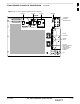
Frame Module Location & Identification – continued 1 Figure 1-8: +27 V SC 4812T Expansion Frame I/O Plate SPAN I/O SITE I/O SPAN I/O LFR/HSO REAR SPAN I/O B TRANSMIT ANTENNA CONNECTORS SPAN I/O A ÄÄÄÄÄÄÄÄÄÄÄÄÄÄÄÄÄÄÄ ÄÄÄÄÄÄÄÄÄÄÄÄÄÄÄÄÄÄÄ ÄÄÄÄÄÄÄÄÄÄÄÄÄÄÄÄÄÄÄ ÄÄÄÄÄÄÄÄÄÄÄÄÄÄÄÄÄÄÄ ÄÄÄÄÄÄÄÄÄÄÄÄÄÄÄÄÄÄÄ ÄÄÄÄÄÄÄÄÄÄÄÄÄÄÄÄÄÄÄ ÄÄÄÄÄÄÄÄÄÄÄÄÄÄÄÄÄÄÄ ÄÄÄÄÄÄÄÄÄÄÄÄÄÄÄÄÄÄÄ ÄÄÄÄÄÄÄÄÄÄÄÄÄÄÄÄÄÄÄ ÄÄÄÄÄÄÄÄÄÄÄÄÄÄÄÄÄÄÄ ÄÄÄÄÄÄÄÄÄÄÄÄÄÄÄÄÄÄÄ ÄÄÄÄÄÄÄÄÄÄÄÄÄÄÄÄÄÄÄ ÄÄÄÄÄÄÄÄÄÄÄÄÄÄÄÄÄÄÄ ÄÄÄÄÄÄÄÄÄÄÄÄÄÄÄÄÄÄÄ ÄÄÄÄÄÄÄÄÄÄÄÄÄÄÄÄÄÄÄ ÄÄÄÄÄÄÄ
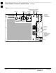
Frame Module Location & Identification – continued Figure 1-9: –48 V SC 4812T Expansion Frame I/O Plate RF FILTER PORTS NOT USED IN EXPANSION FRAME SPAN I/O SITE I/O SPAN I/O HSO/LFR REAR SITE I/O SPAN I/O B SPAN I/O A TRANSMIT ANTENNA CONNECTORS ÄÄÄÄÄÄÄÄÄÄÄÄÄÄÄÄÄÄÄ ÄÄÄÄÄÄÄÄÄÄÄÄÄÄÄÄÄÄÄ ÄÄÄÄÄÄÄÄÄÄÄÄÄÄÄÄÄÄÄ ÄÄÄÄÄÄÄÄÄÄÄÄÄÄÄÄÄÄÄ ÄÄÄÄÄÄÄÄÄÄÄÄÄÄÄÄÄÄÄ ÄÄÄÄÄÄÄÄÄÄÄÄÄÄÄÄÄÄÄ ÄÄÄÄÄÄÄÄÄÄÄÄÄÄÄÄÄÄÄ ÄÄÄÄÄÄÄÄÄÄÄÄÄÄÄÄÄÄÄ ÄÄÄÄÄÄÄÄÄÄÄÄÄÄÄÄÄÄÄ ÄÄÄÄÄÄÄÄÄÄÄÄÄÄÄÄÄÄÄ ÄÄÄÄÄÄÄÄÄÄÄÄÄÄÄÄÄÄÄ ÄÄÄÄÄÄÄÄÄÄÄÄÄÄÄÄÄÄÄ ÄÄÄÄÄÄÄÄÄÄÄÄÄÄÄÄ
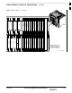
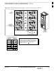
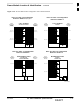
Mar 2001 CCD–1 CIO MCC24–3 MCC24–4 MCC24–5 MCC24–6 BBX2–1 BBX2–2 BBX2–3 BBX2–4 BBX2–5 BBX2–6 BBX2–R MCC24–8 MCC24–9 MCC24–10 MCC24–11 MCC24–12 BBX2–7 BBX2–8 BBX2–9 BBX2–10 BBX2–11 BBX2–12 Switch MPC/EMPC–1 MCC24–2 MCC24–7 MPC/EMPC–2 GLI2–1 MCC24–1 GLI2–2 AMR–1 PS–3 PS–2 PS–1 19 mm Filler Panel AMR–2 38 mm Filler Panel CCD–2 CSM–2 CSM–1 HSO/LFR Frame Module Location & Identification – continued 1 Figure 1-10: SC 4812T C–CCP Shelf SCt4812T CDMA BTS Optimization/ATP ÂÂÂÂÂÂ ÂÂÂÂÂÂ ÂÂÂÂÂÂ
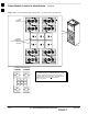
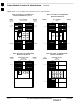
1 Frame Module Location & Identification – continued Figure 1-11: +27 V SC 4812T LPA Configuration – 4 Carrier with 2:1 Combiners FAN MODULE (TYPICAL) LPA1A LPA2A LPA1B LPA2B LPA1C LPA2C LPA1D FILTERS / COMBINERS (2 TO 1 COMBINER SHOWN) LPA2D 1 2 3 4 5 6 FW00296 LPA3A LPA4A LPA3B LPA4B LPA3C LPA4C LPA3D LPA4D 4–CARRIER CONFIGURATION CARRIER CARRIER 1 3 1-26 2 1 2 3 4 5 6 Note No adjacent carriers may exist within the same TX filter combiner.
Frame Module Location & Identification – continued 1 Figure 1-12: –48 V SC 4812T LPA Configuration – 4 Carrier, 3–Sector with 2:1 Combiners LPA1A LPA2A 4 FAN MODULE (TYPICAL) LPA2B LPA1B LPA1C LPA2C 1 LPA1D LPA3A LPA2D LPA4A 5 LPA3B FILTERS / COMBINERS (2 TO 1 COMBINER SHOWN) LPA3C LPA4B LPA4C 2 LPA3D LPA4D 3 –48 Volt SC 4812T 6 FW00481 4–CARRIER CONFIGURATION CARRIER CARRIER 4 1 1 2 Note No adjacent carriers may exist within the same TX filter combiner.
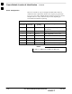
1 Frame Module Location & Identification – continued Sector Configuration There are a number of ways to configure the BTS frame. Table 1-3 outlines the basic requirements. When carrier capacity is greater than two, a 2:1 or 4:1 cavity combiner must be used. For one or two carriers, bandpass filters or cavity combiners may be used, depending on sectorization and channel sequencing.
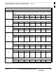
Frame Module Location & Identification – continued 1 Table 1-4: Sector Configurations Config Ref. No. Description 3–Sector/2–ADJACENT Carriers – The configuration below maps TX with optional 2:1 cavity combiners for 3 sectors/2 carriers for adjacent channels. Note that 2:1 cavity combiners are used (6 total).
1 Frame Module Location & Identification – continued Figure 1-13: +27 V SC4812T LPA Configuration with Combiners/Filters Note: See Table 1-4 Configuration Reference Numbers 1, 2, 3, 4. 2 to 1 Combiner Sector Numbering 3 Sector (6 Sector) Sector Numbering 3 Sector (6 Sector) 3 Sector or 6 Sector LPA 1A C1, S1–3 (C1, S1–3) Note: See Table 1-4 Configuration Reference Number 6.
Frame Module Location & Identification – continued 1 Figure 1-14: –48 V SC4812T LPA Configuration with Combiners/Filters Note: See Table 1-4 Configuration Reference Numbers 1, 2, 3, 4.
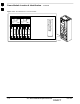
Frame Module Location & Identification – continued Figure 1-15: –48 V BTS Power Conversion Shelf FAN MODULE REAR FAN MODULE REAR FRONT PWR/ALM 1A 30 1B 1C 30 1D PWR/ALM FRONT 2A 30 PS–9 PS–8 PS–7 PS–6 PS–5 PS–4 L 2C P A 3A AMR 1 30 2B 2D 30 3B 3C 30 3D 4A 30 4B 4C 30 4D FW00501 1-32 SCt4812T CDMA BTS Optimization/ATP Mar 2001 DRAFT
Frame Module Location & Identification – continued 1 Figure 1-16: CDMA (COBRA) RFDS Layout FRONT VIEW POWER SUPPLY ON/OFF ROCKER SWITCH CASU 1 CASU 2 MMI PORT AND PWR/ALARM LED ESN LABEL (FOR SC 6XX SERIES BTS) FWTIC Cobra RFDS external housing (Shown With Cover off) SUA ESN LABEL (FOR SC XXXX SERIES BTS) LEDS MMI Cobra RFDS Field Replaceable Unit (FRU) (shown removed from external housing) CHASSIS GND ELECTRICAL GND Cobra RFDS RF connector panel detail (shown from rear) FW00138 POWER CONNECTO
1 Frame Module Location & Identification – continued Notes 1-34 SCt4812T CDMA BTS Optimization/ATP Mar 2001 DRAFT
Chapter 2: Preliminary Operations Table of Contents Mar 2001 Preliminary Operations: Overview . . . . . . . . . . . . . . . . . . . . . . . . . . . . . . . . . . . Introduction . . . . . . . . . . . . . . . . . . . . . . . . . . . . . . . . . . . . . . . . . . . . . . Cell Site Types . . . . . . . . . . . . . . . . . . . . . . . . . . . . . . . . . . . . . . . . . . . . CDF . . . . . . . . . . . . . . . . . . . . . . . . . . . . . . . . . . . . . . . . . . . . . . . . . . . . Site Equipage Verification .
Table of Contents – continued Notes 2 SCt4812T CDMA BTS Optimization/ATP Mar 2001 DRAFT
Preliminary Operations: Overview Introduction This section first verifies proper frame equipage. This includes verifying module placement, jumper, and dual in–line package (DIP) switch settings against the site-specific documentation supplied for each BTS application. Next, pre-power up and initial power-up procedures are presented. Cell Site Types Sites are configured as Omni with a maximum of 4 carriers, 3–sectored with a maximum of 4 carriers, and 6–sectored with a maximum of 2 carriers.
Preliminary Operations: Overview – continued Table 2-1: Initial Installation of Boards/Modules Step 2 1 Action Refer to the site documentation and install all boards and modules into the appropriate shelves as required. Verify they are NOT SEATED at this time. NOTE On 800 MHz systems, the Switch Card has a configuration switch that must match the site configuration (see Figure 2-1).
Preliminary Operations: Overview – continued Setting Frame C–CCP Shelf Configuration Switch The backplane switch settings behind the fan module nearest the breaker panel should be set as shown in Figure 2-2. The switch setting must be verified and set before power is applied to the BTS equipment.
Pre–Power–up Tests Objective 2 This procedure checks for any electrical short circuits and verifies the operation and tolerances of the cellsite and BTS power supply units prior to applying power for the first time. Test Equipment The following test equipment is required to complete the pre–power–up tests: Digital Multimeter (DMM) CAUTION Always wear a conductive, high impedance wrist strap while handling the any circuit card/module to prevent damage by ESD.
Pre–Power–up Tests – continued DC Power Pre-test (BTS Frame) Before applying any power to the BTS frame, follow the procedure in Table 2-2 while referring to Figure 2-3 and Figure 2-4 for +27 V systems or to Figure 2-5 and Figure 2-6 for –48 V systems to verify there are no shorts in the BTS frame DC distribution system. 2 Table 2-2: DC Power Pre–test (BTS Frame) Step Action 1 Physically verify that all DC power sources supplying power to the frame are OFF or disabled.
Pre–Power–up Tests – continued Table 2-2: DC Power Pre–test (BTS Frame) Step 2 7 Action Set the LPA breakers ON by pushing them IN one at a time. Repeat Step 3 after turning on each breaker. A typical response is that the ohmmeter will steadily climb in resistance as capacitors charge, stopping at approximately 500 Ω.. 8 In the –48 V BTS, insert and lock the DC/DC LPA converter modules into their associated slots one at a time. Repeat Step 3 after inserting each module.
Pre–Power–up Tests – continued Figure 2-3: +27 V BTS DC Distribution Pre-test TOP OF FRAME 2C 30 2D 3A 30 3B 3C 30 3D 4A 30 4B 4C 30 4D 1 50 2 50 3 50 4 2B 1 30 5 2A 2 1D 6 30 LIVE TERMINALS 3 1C +27 VDC GND L P A 1B CAUTION LPA BREAKERS 30 LFR/ HSO LIVE TERMINALS 1A 2 TX OUT FW00298 POWER INPUT C–CCP BREAKERS C C C P BREAKER PANEL Breakering: Two LPAs on each trunking backplane breakered together Designed for peak LPA current of 15 amps (30 amp breake
Pre–Power–up Tests – continued Figure 2-4: +27 V SC 4812T BTS Starter Frame Span I/O A RGD (Needed for Expansion only) 2 Site I/O ÂÂÂÂÂÂÂÂÂÂÂÂ ÂÂÂÂÂÂÂÂÂÂÂÂ ÂÂÂÂÂÂÂÂÂÂÂÂ ÂÂÂÂÂÂÂÂÂÂÂÂ ÂÂÂÂÂÂÂÂÂÂÂÂ ÂÂÂÂÂÂÂÂÂÂÂÂ ÂÂÂÂÂÂÂÂÂÂÂÂ Á Span I/O B Exhaust Region RX In (1A – 6A and 1B – 6B) TX Out (1 – 6) Power Input Connection C–CCP Cage ÁÁ Á Expansion I/O Housing Á Á Breakers Front Cosmetic Panel LPA Cage Combiner Section For clarity, doors are not shown.
Pre–Power–up Tests – continued Figure 2-5: –48 V BTS DC Distribution Pre-test TOP OF FRAME LIVE TERMINALS WIRED FOR –48 VDC 2 LIVE TERMINALS HSO/ LFR 3 2 1 3 2 1 1 5 4 6 2 3 GND CAUTION TX OUT P O W E R 1 30 4 40 5 40 2 30 6 40 7 40 3 POWER INPUT L P A 30 8 40 9 40 C–CCP BREAKER 1A 30 1B 1C 30 1D 2A 30 2B 2C 30 2D 3A 30 3B 3C 30 3D 4A 30 4B 4C 30 4D LPA BREAKER Breakering: Two LPAs on each trunking backplane breakered together Designed f
Pre–Power–up Tests – continued Figure 2-6: –48 V SC 4812T BTS Starter Frame Alarms RGD (Needed for Expansion only) 2 ÂÂÂÂÂÂÂÂÂÂ ÂÂÂÂÂÂÂÂÂÂ ÂÂÂÂÂÂÂÂÂÂ ÂÂÂÂÂÂÂÂÂÂ ÂÂÂÂÂÂÂÂÂÂ ÂÂÂÂÂÂÂÂÂÂ ÂÂÂÂÂÂÂÂÂÂ Á ÁÁ Á ÁÁ Á Exhaust Region C–CCP Cage Span I/O A Site I/O Span I/O B RX In (1A – 6A and 1B – 6B) TX Out (1 – 6) Power Input Connection Expansion I/O Housing Breakers Front Cosmetic Panel LPA Cage Combiner Section Power Conversion Shelf Á Breakers For clarity, doors are not shown.
Pre–Power–up Tests – continued DC Power Pre-test (RFDS) Before applying power to the RFDS, follow the steps in Table 2-3, while referring to Figure 2-7, to verify there are no shorts in the RFDS DC distribution system, backplanes, or modules/boards. As of the date of this publication, the RFDS is not used with the –48 V BTS. IMPORTANT * Visual inspection of card placement and equipage for each frame vs.
Initial Power–up Tests Power-up Procedures 2 WARNING Potentially lethal voltage and current levels are routed to the BTS equipment. This test must be performed with a second person present, acting in a safety role. Remove all rings, jewelry, and wrist watches prior to beginning this test. DC Input Power In the tests to follow, power will first be verified at the input to each BTS frame. After power is verified, cards and modules within the frame itself will be powered up and verified one at a time.
Initial Power–up Tests – continued Table 2-4: DC Input Power Cable Guidelines Maximum Cable Length Wire Size 30.38 m (100 ft) 107 mm2 (AWG #4/0) 54.864 m (180 ft) 185 mm2 (350 kcmil) Greater that 54.864 m (180 ft) Not recommended 2 IMPORTANT * If Anderson SB350 style power connectors are used, make sure the connector adapters are securely attached to each of the BTS power feeds and returns. Also, make sure the cables have been properly installed into each connector.
Initial Power–up Tests – continued Initial Power-up (RFDS) The procedure in Table 2-6 must be performed on the RFDS after input power from the common power supply has been verified. Perform the following steps to apply initial power to the cards/modules within the frame itself, verifying that each is operating within specification. 2 IMPORTANT * Visual inspection of card placement and equipage for each frame vs.
Initial Power–up Tests – continued Table 2-7: Initial Power–up (BTS) Step 5 Action Seat the first equipped LPA module pair into the assigned slot in the upper LPA shelf including LPA fan. In +27 V systems, observe that the LPA internal fan comes on line. 6 Repeat step 5 for all remaining LPAs. 7 Set the LPA breakers to the ON position (per configuration) by pushing them IN one at a time.
Initial Power–up Tests – continued Notes 2 2-16 SCt4812T CDMA BTS Optimization/ATP Mar 2001 DRAFT
Chapter 3: Optimization/Calibration Table of Contents 3 Mar 2001 Optimization/Calibration – Introduction . . . . . . . . . . . . . . . . . . . . . . . . . . . . . . Introduction . . . . . . . . . . . . . . . . . . . . . . . . . . . . . . . . . . . . . . . . . . . . . . Optimization Process . . . . . . . . . . . . . . . . . . . . . . . . . . . . . . . . . . . . . . . Cell Site Types . . . . . . . . . . . . . . . . . . . . . . . . . . . . . . . . . . . . . . . . . . . . Cell–Site Data File . . . . . . . .
Table of Contents 3 – continued Null Modem Cable . . . . . . . . . . . . . . . . . . . . . . . . . . . . . . . . . . . . . . . . CSM Frequency Verification . . . . . . . . . . . . . . . . . . . . . . . . . . . . . . . . . Test Equipment Setup: GPS & LFR/HSO Verification . . . . . . . . . . . . . GPS Initialization/Verification . . . . . . . . . . . . . . . . . . . . . . . . . . . . . . . . LFR Initialization/Verification . . . . . . . . . . . . . . . . . . . . . . . . . . . . . . . .
Table of Contents Mar 2001 – continued Set Antenna Map Data . . . . . . . . . . . . . . . . . . . . . . . . . . . . . . . . . . . . . . Set RFDS Configuration Data . . . . . . . . . . . . . . . . . . . . . . . . . . . . . . . . RFDS Calibration . . . . . . . . . . . . . . . . . . . . . . . . . . . . . . . . . . . . . . . . . Program TSU NAM . . . . . . . . . . . . . . . . . . . . . . . . . . . . . . . . . . . . . . . . 3-80 3-81 3-82 3-83 BTS Redundancy/Alarm Testing . . . . . . . . . . . . . . . . . .
Table of Contents – continued Notes 3 SCt4812T CDMA BTS Optimization/ATP Mar 2001 DRAFT
Optimization/Calibration – Introduction Introduction This section describes procedures for isolating the BTS from the span lines, preparing and using the LMF, downloading system operating software, CSM reference verification/optimization, set up and calibration of the supported test equipment, transmit/receive path verification, using the RFDS, and verifying the customer defined alarms and relay contacts are functioning properly.
Optimization/Calibration – Introduction – continued 10. Select all of the BBXs and all of the MCCs, and use the full optimization function. The full optimization function performs TX calibration, BLO download, TX audit, all TX tests, and all RX tests for all selected devices. 11. If the TX calibration fails, repeat the full optimization for any failed paths. 12. If the TX calibration fails again, correct the problem that caused the failure and repeat the full optimization for the failed path. 3 13.
Optimization/Calibration – Introduction – continued Effective Rated Power (ERP) table for all TX channels to antennas respectively. Motorola System Engineering specifies the ERP of a transmit antenna based on site geography, antenna placement, and government regulations. Working from this ERP requirement, the antenna gain, (dependent on the units of measurement specified) and antenna feed line loss can be combined to determine the required power at the top of the BTS frame.
Isolate Span Lines/Connect LMF Isolate BTS from T1/E1 Spans IMPORTANT * 3 At active sites, the OMC/CBSC must disable the BTS and place it out of service (OOS). DO NOT remove the 50–pin TELCO cable connected to the BTS frame site I/O board J1 connector until the OMC/CBSC has disabled the BTS! Each frame is equipped with one Site I/O and two Span I/O boards. The Span I/O J1 connector provides connection of 25 pairs of wire. A GLI2 card can support up to six spans.
Isolate Span Lines/Connect LMF – continued Figure 3-1: Span I/O Board T1 Span Isolation 50–PIN TELCO CONNECTORS REMOVED SPAN A CONNECTOR (TELCO) INTERFACE TO SPAN LINES 3 SPAN B CONNECTOR (TELCO) INTERFACE TO SPAN LINES RS–232 9–PIN SUB D CONNECTOR SERIAL PORT FOR EXTERNAL DIAL UP MODEM CONNECTION (IF USED) TOP of Frame (Site I/O and Span I/O boards) FW00299 LMF to BTS Connection The LMF is connected to the LAN A or B connector located on the left side of the frame’s lower air intake grill, behind the
Isolate Span Lines/Connect LMF – continued Figure 3-2: LMF Connection Detail NOTE: Open LAN CABLE ACCESS door. Pull apart Velcro tape and gain access to the LAN A or LAN B LMF BNC connector.
Preparing the LMF Overview Software and files for installation and updating of the LMF are provided on CD ROM disks. The following installation items must be available: LMF Program on CD ROM LMF Binaries on CD ROM CDF for each supported BTS (on diskette or available from the 3 CBSC) CBSC File for each supported BTS (on diskette or available from the CBSC) The following section provides information and instructions for installing and updating the LMF software and files.
Preparing the LMF – continued Table 3-3: LMF Operating System Installation Step 5 Action Follow the instructions displayed on the Setup screen.
Preparing the LMF – continued IMPORTANT * When copying CDF files, comply with the following to prevent BTS login problems with the LMF: – The numbers used in the bts–#.cdf and cbsc–#.cdf filenames must correspond to the locally assigned numbers for each BTS and its controlling CBSC. – The generic cbsc–1.cdf file supplied with the LMF work with locally numbered BTS CDF files. Using this file does not provide a valid optimization unless the generic file is edited to replace default parameters (e.g.
Preparing the LMF – continued Table 3-4: Copying CBSC CDF Files to the LMF Step 3 Action 8 Repeat steps 5 through 7 for each bts–# that must be supported by the LMF. 9 When all required files have been copied to the diskette, type eject and press the key. 10 Remove the diskette from the CBSC. AT THE LMF: 11 Start the Windows operating system. 12 Insert the diskette into the LMF. 13 Using Windows Explorer (or equivalent program), create a corresponding bts–# folder in the wlmf\cdma
Preparing the LMF – continued Table 3-5: Creating a Named Hyperlink Connection for MMI Connection Step Action 1 From the Windows Start menu, select: Programs>Accessories 2 Perform one of the following: For Win NT, select Hyperterminal and then click on HyperTerminal For Win 98, select Communications, double click the Hyperterminal folder, and then double click on the Hyperterm.exe icon in the window that opens.
Preparing the LMF – continued Table 3-5: Creating a Named Hyperlink Connection for MMI Connection Step 10 Action Perform one of the following: If the Hyperterminal folder window is still open (Win 98) proceed to step 12 From the Windows Start menu, select Programs > Accessories 11 3 Perform one of the following: For Win NT, select Hyperterminal and release any pressed mouse buttons. For Win 98, select Communications and double click the Hyperterminal folder.
Preparing the LMF – continued Folder Structure Overview The LMF uses a wlmf folder that contains all of the essential data for installing and maintaining the BTS. The list that follows outlines the folder structure for the LMF. Except for the bts–nnn folders, these folders are created as part of the the LMF installation. Refer to the CDMA LMF Operator’s Guide for a complete description of the folder structure.
Preparing the LMF – continued Pinging the Processors For proper operation, the integrity of the Ethernet LAN A and B links must be be verified. Figure 3-4 represents a typical BTS Ethernet configuration. The drawing depicts one (of two identical) links, A and B. Ping is a program that routes request packets to the LAN network modules to obtain a response from the specified “targeted” BTS.
Preparing the LMF – continued Table 3-6: Pinging the Processors Step Action 1 If you have not already done so, connect the LMF to the BTS (see Table 3-2 on page 3-5). 2 From the Windows desktop, click the Start button and select Run. 3 In the Open box, type ping and the (for example, ping 128.0.0.2). NOTE 128.0.0.2 is the default IP address for MGLI–1 in field BTS units. 128.0.0.1 is the default IP address for MGLI–2. 4 Click on the OK button.
Preparing the LMF – continued Figure 3-5: +27 V SC 4812T Starter Frame I/O Plate ALARM B SPAN I/O B SITE I/O TOP VIEW 3-16 SCt4812T CDMA BTS Optimization/ATP 5 3 6 2B GND RX 3A 3B 4A 4B 5A 5B 6A 6B CAUTION EXP I/O FRONT 2 LFR/ HSO LIVE TERMINALS SPAN I/O A 2A 1B 4 +27 VDC RGD 3 RGPS 1A 1 LIVE TERMINALS ÄÄÄÄÄÄÄÄÄÄÄÄÄÄÄÄÄÄÄ ÄÄÄÄÄÄÄÄÄÄÄÄÄÄÄÄÄÄÄ ÄÄÄÄÄÄÄÄÄÄÄÄÄÄÄÄÄÄÄ ÄÄÄÄÄÄÄÄÄÄÄÄÄÄÄÄÄÄÄ ÄÄÄÄÄÄÄÄÄÄÄÄÄÄÄÄÄÄÄ ÄÄÄÄÄÄÄÄÄÄÄÄÄÄÄÄÄÄÄ ÄÄÄÄÄÄÄÄÄÄÄÄÄÄÄÄÄÄÄ ÄÄÄÄÄÄÄÄÄÄÄÄÄÄÄÄÄÄÄ ÄÄÄÄÄÄÄÄÄÄ