X UBS Macro BTS Optimization/ATP Acceptance Test Procedures - TX & RX Perform the procedure in Procedure 4-6 for all-inclusive RX test. Procedure 4-6 All RX ATP Test 1 Set up the test equipment for abbreviated acceptance tests per Procedure 4-3 2 On LMF, select devices to be tested. To select multiple items, hold down the Shift or Ctrl key while making the selections. 3 Click on Tests in the UBS Menu bar, and select All RX Test... from pull-down menu.
Individual Tests Chapter 4: Acceptance Test Procedures Individual Tests ■ ■ ■ ■ ■ ■ ■ ■ ■ ■ ■ ■ ■ ■ ■ ■ ■ ■ ■ ■ ■ ■ ■ ■ ■ ■ ■ ■ ■ ■ ■ ■ ■ ■ ■ ■ ■ ■ ■ ■ ■ ■ ■ ■ ■ ■ ■ ■ ■ ■ ■ ■ ■ ■ ■ ■ ■ ■ ■ ■ ■ ■ ■ ■ TX and RX Testing The following individual ATP tests can be used to evaluate specific aspects of UBS operation against individual performance requirements. All testing is performed using the LMF GUI environment.
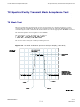
1X UBS Macro BTS Optimization/ATP Individual Tests Waveform Quality (Rho) This test verifies the transmitted Pilot channel element digital waveform quality of each sector-carrier enabled at a specific frequency per the current NEC file assignment. All tests are performed using the external calibrated test set controlled by the same command. All measurements are via the appropriate TX OUT connector.
Individual Tests Chapter 4: Acceptance Test Procedures Receive Signal Strength Indication (RSSI) This test verifies the gain for UBS reverse (RX) paths for each carrier-sector selected is within requirements for correct operation for the operating band of the UBS as follows: • 1900 MHz: –80 dBm (-86 dBm or greater) • 800 MHz: –80 dBm (-86 dBm or greater) The LMF injects a -80 dBm signal (default) input to the UBS. The RSSI must be +/-6 dB.
1X UBS Macro BTS Optimization/ATP TX Spectral Purity Transmit Mask Acceptance Test TX Spectral Purity Transmit Mask Acceptance Test ■ ■ ■ ■ ■ ■ ■ ■ ■ ■ ■ ■ ■ ■ ■ ■ ■ ■ ■ ■ ■ ■ ■ ■ ■ ■ ■ ■ ■ ■ ■ ■ ■ ■ ■ ■ ■ ■ ■ ■ ■ ■ ■ ■ ■ ■ ■ ■ ■ ■ ■ ■ ■ ■ ■ ■ ■ ■ ■ ■ ■ ■ ■ ■ TX Mask Test This test verifies the spectral purity of each sector-carrier at a specific frequency, per the current NEC file assignment.
TX Waveform Quality (Rho) Acceptance Test Chapter 4: Acceptance Test Procedures TX Waveform Quality (Rho) Acceptance Test ■ ■ ■ ■ ■ ■ ■ ■ ■ ■ ■ ■ ■ ■ ■ ■ ■ ■ ■ ■ ■ ■ ■ ■ ■ ■ ■ ■ ■ ■ ■ ■ ■ ■ ■ ■ ■ ■ ■ ■ ■ ■ ■ ■ ■ ■ ■ ■ ■ ■ ■ ■ ■ ■ ■ ■ ■ ■ ■ ■ ■ ■ ■ ■ Rho Test The Pilot Gain is set to 171 for each antenna.
1X UBS Macro BTS Optimization/ATP TX Pilot Time Offset Acceptance Test TX Pilot Time Offset Acceptance Test ■ ■ ■ ■ ■ ■ ■ ■ ■ ■ ■ ■ ■ ■ ■ ■ ■ ■ ■ ■ ■ ■ ■ ■ ■ ■ ■ ■ ■ ■ ■ ■ ■ ■ ■ ■ ■ ■ ■ ■ ■ ■ ■ ■ ■ ■ ■ ■ ■ ■ ■ ■ ■ ■ ■ ■ ■ ■ ■ ■ ■ ■ ■ ■ PTO Acceptance Test This test verifies the transmitted Pilot channel element Pilot Time Offset of each sector-carrier keyed up at a specific frequency per the current NEC file assignment.
TX Pilot Time Offset Acceptance Test Figure 4-5 Chapter 4: Acceptance Test Procedures Pilot Only Signal ti-cdma-pilot_only.
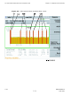
1X UBS Macro BTS Optimization/ATP TX Code Domain Power/Noise Floor Acceptance Test TX Code Domain Power/Noise Floor Acceptance Test ■ ■ ■ ■ ■ ■ ■ ■ ■ ■ ■ ■ ■ ■ ■ ■ ■ ■ ■ ■ ■ ■ ■ ■ ■ ■ ■ ■ ■ ■ ■ ■ ■ ■ ■ ■ ■ ■ ■ ■ ■ ■ ■ ■ ■ ■ ■ ■ ■ ■ ■ ■ ■ ■ ■ ■ ■ ■ ■ ■ ■ ■ ■ ■ Code Domain Power Test For each sector/antenna under test, the Pilot Gain is set to 383 LSB.
TX Code Domain Power/Noise Floor Acceptance Test Chapter 4: Acceptance Test Procedures Figure 4-6 Code Domain Power and Noise Floor Levels PILOT PAGING TRAFFIC SYNC TRAFFIC ti-cdma-standa rd_pa ttern.
1X UBS Macro BTS Optimization/ATP RX Frame Error Rate (FER) Acceptance Test RX Frame Error Rate (FER) Acceptance Test ■ ■ ■ ■ ■ ■ ■ ■ ■ ■ ■ ■ ■ ■ ■ ■ ■ ■ ■ ■ ■ ■ ■ ■ ■ ■ ■ ■ ■ ■ ■ ■ ■ ■ ■ ■ ■ ■ ■ ■ ■ ■ ■ ■ ■ ■ ■ ■ ■ ■ ■ ■ ■ ■ ■ ■ ■ ■ ■ ■ ■ ■ ■ ■ FER Test This test verifies the UBS FER on all traffic channel elements is currently configured (full rate at 1% FER) at an RF input level of -123 dBm.
Continuous Waveform Mode Chapter 4: Acceptance Test Procedures Continuous Waveform Mode ■ ■ ■ ■ ■ ■ ■ ■ ■ ■ ■ ■ ■ ■ ■ ■ ■ ■ ■ ■ ■ ■ ■ ■ ■ ■ ■ ■ ■ ■ ■ ■ ■ ■ ■ ■ ■ ■ ■ ■ ■ ■ ■ ■ ■ ■ ■ ■ ■ ■ ■ ■ ■ ■ ■ ■ ■ ■ ■ ■ ■ ■ ■ ■ Objective This test verifies that the UBS frames can generate an unmodulated carrier tone on a single sector at any single channel number within the supported carrier frequency range of the frame.
1X UBS Macro BTS Optimization/ATP Continuous Waveform Mode Lock Continuous Waveform Mode Procedure 4-8 Procedure to Lock Continuous Waveform Mode 1 On the menu, click on UBS -> Lock Continuous Waveform Mode 2 A status report window will appear that shows the result of the action request. WinLMF will fail to disable Continuous Waveform Mode for Modem devices provisioned in the conguration les on DMI, but not physically installed in the frame and for Modem devices under reset.
Generate ATP Report Chapter 4: Acceptance Test Procedures Generate ATP Report ■ ■ ■ ■ ■ ■ ■ ■ ■ ■ ■ ■ ■ ■ ■ ■ ■ ■ ■ ■ ■ ■ ■ ■ ■ ■ ■ ■ ■ ■ ■ ■ ■ ■ ■ ■ ■ ■ ■ ■ ■ ■ ■ ■ ■ ■ ■ ■ ■ ■ ■ ■ ■ ■ ■ ■ ■ ■ ■ ■ ■ ■ ■ ■ Background Each time an Acceptance Test Procedure (ATP) report is updated to include the results of the most recent ATP tests if the Save Results button is used to close the status report window.
1X UBS Macro BTS Optimization/ATP Procedure 4-9 Generate ATP Report Generating an ATP Report 1 Click Util. Save Test Report from the LMF menu. 2 Click on a column heading to sort the report. 3 Do one of the following: • If a printable file copy is not desired, click on the Dismiss button. • If a printable copy is required, select the desired file type in the pick list and click on the Save button.
Generate ATP Report Chapter 4: Acceptance Test Procedures 4-28 68P09283A63-5 FOA AUG 2007
Chapter 5 Leave the Site ■ ■ ■ ■ ■ ■ ■ ■ ■ ■ ■ ■ ■ ■ ■ ■ ■ ■ ■ ■ ■ ■ ■ ■ ■ ■ ■ ■ ■ ■ ■ ■ ■ ■ ■ ■ ■ ■ ■ ■ ■ ■ ■ ■ ■ ■ ■ ■ ■ ■ ■ ■ ■ ■ ■ ■ ■ ■ ■ ■ ■ ■ ■ ■ ■ ■ 68P09283A63-5 AUG 2007 5-1 FOA
Conguring Backhaul Chapter 5: Leave the Site Conguring Backhaul ■ ■ ■ ■ ■ ■ ■ ■ ■ ■ ■ ■ ■ ■ ■ ■ ■ ■ ■ ■ ■ ■ ■ ■ ■ ■ ■ ■ ■ ■ ■ ■ ■ ■ ■ ■ ■ ■ ■ ■ ■ ■ ■ ■ ■ ■ ■ ■ ■ ■ ■ ■ ■ ■ ■ ■ ■ ■ ■ ■ ■ ■ ■ ■ Before disconnecting the LMF and test equipment, the span backhaul must be configured to allow the UBS to communicate with the OMC-R.
1X UBS Macro BTS Optimization/ATP Conguring Backhaul Figure 5-1 Congure Backhaul Basic Screen ti-cdma-06184.eps Procedure 5-1 Fractional Span Backhaul Conguration Procedure 1 Go to the LMF Configure Backhaul Screen. See Figure 5-1 The default value for both the LcpNcpNegRetryInt and the PPPKeepAliveMsg parameters is 1000 ms. If the UBS will use satellite backhaul, the value for these parameters must be set to 2000 ms.
Conguring Backhaul Chapter 5: Leave the Site Using the LMF Congure Backhaul Advanced Screen In the event that a backhaul configuration entered at the Operation and maintenance Center-Radio (OMC-R) results in the OMC-R being unable to communicate with the BTS, it may be necessary to reset backhaul parameters to their default values using the LMF. The LMF Configure Backhaul Advanced Screen is used to reset these values.
1X UBS Macro BTS Optimization/ATP Conguring Backhaul Span configuration (ubsSpan) • Span type: T1 • Frame type: ESF, Extended ... • Coding type: B8ZS, Bipolar 8–... • Termination type: TX131, 131 to 2...
Conguring Backhaul Chapter 5: Leave the Site Figure 5-2 Congure Backhaul Advanced Screen en ter_filena me_her e_and_mo ve_per_st ep_8 5-6 68P09283A63-5 FOA AUG 2007
1X UBS Macro BTS Optimization/ATP Prepare to Leave the Site Prepare to Leave the Site ■ ■ ■ ■ ■ ■ ■ ■ ■ ■ ■ ■ ■ ■ ■ ■ ■ ■ ■ ■ ■ ■ ■ ■ ■ ■ ■ ■ ■ ■ ■ ■ ■ ■ ■ ■ ■ ■ ■ ■ ■ ■ ■ ■ ■ ■ ■ ■ ■ ■ ■ ■ ■ ■ ■ ■ ■ ■ ■ ■ ■ ■ ■ ■ External Test Equipment Removal Perform the procedure in Procedure 5-3 to disconnect the test equipment and configure the UBS for active service.
Prepare to Leave the Site Chapter 5: Leave the Site Procedure 5-4 1 LMF Termination and Removal Procedure From the Local Terminal window select File > Exit. Anytime the LMF is exited from the UBS, the DMI controller(s) will automatically reboot within 1 minute in order to clear out any test configurations and boot up under the original configuration in the NECB and NECJ files. 2 From the Windows Task Bar click Start > Shutdown. Click Yes when the Shut Down Windows message appears.
Appendix A Data Sheets 68P09283A63-5 AUG 2007 A-1 FOA
Optimization/ATP Checklist Appendix A: Data Sheets Optimization/ATP Checklist ■ ■ ■ ■ ■ ■ ■ ■ ■ ■ ■ ■ ■ ■ ■ ■ ■ ■ ■ ■ ■ ■ ■ ■ ■ ■ ■ ■ ■ ■ ■ ■ ■ ■ ■ ■ ■ ■ ■ ■ ■ ■ ■ ■ ■ ■ ■ ■ ■ ■ ■ ■ ■ ■ ■ ■ ■ ■ ■ ■ ■ ■ ■ ■ Verication of Test Equipment Used Table A-1 Test Equipment Used Checklist Manufacturer Model Serial Number A-2 68P09283A63-5 FOA AUG 2007
1X UBS Macro BTS Optimization/ATP Optimization/ATP Checklist Checklist Table A-2 Procedure Checklist Parameter Specication Comments Power Up Procedures Pre-Power Up Test Per Procedure 2-1 Initial Power Up Test Per Procedure 2-2 andProcedure 2-3 Optimization/ATP Procedures LMF-to-UBS Connection Per Procedure 3-2 UBS GUI Login Per Procedure 3-3 UBS GUI Logout Per Procedure 3-4 Generate ATP Report Per Procedure 4-9 Leave the Site Test Equipment Removal Per Procedure 5-3, Procedure 5-5 Reset
A-4 68P09283A63-5 FOA AUG 2007
Appendix B FRU Optimization/ATP Matrix 68P09283A63-5 AUG 2007 B-1 FOA
FRU Optimization/ATP Test Matrix Appendix B: FRU Optimization/ATP Matrix FRU Optimization/ATP Test Matrix ■ ■ ■ ■ ■ ■ ■ ■ ■ ■ ■ ■ ■ ■ ■ ■ ■ ■ ■ ■ ■ ■ ■ ■ ■ ■ ■ ■ ■ ■ ■ ■ ■ ■ ■ ■ ■ ■ ■ ■ ■ ■ ■ ■ ■ ■ ■ ■ ■ ■ ■ ■ ■ ■ ■ ■ ■ ■ ■ ■ ■ ■ ■ ■ Usage & Background Re-optimization of specific portions of the site may be required. An outline of some basic guidelines is included in the following tables.
1X UBS Macro BTS Optimization/ATP FRU Optimization/ATP Test Matrix Not every procedure required to bring the site back on line is indicated in Table B-2. It is meant to be used as a guideline ONLY. The table assumes that the user is familiar enough with the UBS Optimization/ATP procedure to understand which test equipment set ups, test set calibrations, and UBS site preparation will be required before performing the Table # procedures referenced.
B-4 68P09283A63-5 FOA AUG 2007
Appendix C CDMA Operating Frequency 68P09283A63-5 AUG 2007 C-1 FOA
800 MHz CDMA Operating Frequency Programming Information Appendix C: CDMA Operating Frequency 800 MHz CDMA Operating Frequency Programming Information ■ ■ ■ ■ ■ ■ ■ ■ ■ ■ ■ ■ ■ ■ ■ ■ ■ ■ ■ ■ ■ ■ ■ ■ ■ ■ ■ ■ ■ ■ ■ ■ ■ ■ ■ ■ ■ ■ ■ ■ ■ ■ ■ ■ ■ ■ ■ ■ ■ ■ ■ ■ ■ ■ ■ ■ ■ ■ ■ ■ ■ ■ ■ ■ Introduction Programming of each of the BTS XMIs is performed by the BTS DMI modules over the Concentration Highway Interface (CHI) bus.
1X UBS Macro BTS Optimization/ATP 800 MHz CDMA Operating Frequency Programming Information Table C-1 800 MHz Channel Allocations (Continued) System Designator China CDMA Channel Validity Valid Channel No. 37–283 RX (MHz) 826.11–833.49 TX (MHz) 871.11–878.49 The UBS supports all valid channels within the 800 MHz band and two Conditionally Valid channels: 1019 and 1020. On any other conditionally valid channels within the 800 MHz band, full TX Output power cannot be supported.
800 MHz CDMA Operating Frequency Programming Information Appendix C: CDMA Operating Frequency Figure C-1 800 MHz Frequency Spectrum (CDMA Allocation) F R E Q U E N C Y IN C R E AS E RX (MHz) CHANNELS TX 824.700 824.880 824.910 825.000 825.030 869.700 869.880 869.910 870.000 870.030 1013 1019 1020 1023 1 825.110 870.110 37 833.490 878.490 283 834.090 834.120 834.330 879.090 879.120 897.330 303 304 835.680 880.680 356 835.860 835.890 880.860 880.890 362 363 844.110 844.140 889.
1X UBS Macro BTS Optimization/ATP 800 MHz CDMA Operating Frequency Programming Information 800 MHz Channel Center Frequencies Table C-2 shows the valid 800 MHz CDMA channels, listed in both decimal and hexadecimal, and the corresponding transmit and receive frequency for each. Actual frequencies used depend on customer CDMA system frequency plan. Other channels and frequencies can be calculated using the following formula: For channels 1–799: • TX Freq = 870.00 + (0.03 x Channel) • RX Freq = (0.
1900 MHz CDMA Operating Frequency Programming Information Appendix C: CDMA Operating Frequency 1900 MHz CDMA Operating Frequency Programming Information ■ ■ ■ ■ ■ ■ ■ ■ ■ ■ ■ ■ ■ ■ ■ ■ ■ ■ ■ ■ ■ ■ ■ ■ ■ ■ ■ ■ ■ ■ ■ ■ ■ ■ ■ ■ ■ ■ ■ ■ ■ ■ ■ ■ ■ ■ ■ ■ ■ ■ ■ ■ ■ ■ ■ ■ ■ ■ ■ ■ ■ ■ ■ ■ Introduction Programming of each of the BTS XMIs is performed by the BTS DMI modules over the Concentration Highway Interface (CHI) bus.
1X UBS Macro BTS Optimization/ATP 1900 MHz CDMA Operating Frequency Programming Information Figure C-2 1900 MHz Frequency Spectrum (CDMA Allocation) F R E Q U E N C Y IN C R E AS E RX (MHz) CHANNELS TX 1851.25 1931.25 25 1855.00 1935.00 100 1860.00 1940.00 200 1867.50 1947.50 350 1872.50 1952.50 450 1876.25 1956.25 525 1882.50 1962.50 650 1887.50 1967.50 750 1891.25 1971.25 825 1895.00 1975.00 900 1902.50 1982.50 1050 1905.00 1985.00 1100 1908.75 1988.
1900 MHz CDMA Operating Frequency Programming Information Appendix C: CDMA Operating Frequency 1900 MHz Channel Center Frequencies Table C-4 shows some of the valid 1900 MHz CDMA channels, listed in both decimal and hexadecimal, and the corresponding transmit and receive frequency for each. Actual frequencies used depend on customer CDMA system frequency plan. Other channels and frequencies can be calculated using the following formula: For channels 0–1199: • TX Freq = 1930.00 + (0.
1X UBS Macro BTS Optimization/ATP CDMA Operating Frequency Programming Information CDMA Operating Frequency Programming Information ■ ■ ■ ■ ■ ■ ■ ■ ■ ■ ■ ■ ■ ■ ■ ■ ■ ■ ■ ■ ■ ■ ■ ■ ■ ■ ■ ■ ■ ■ ■ ■ ■ ■ ■ ■ ■ ■ ■ ■ ■ ■ ■ ■ ■ ■ ■ ■ ■ ■ ■ ■ ■ ■ ■ ■ ■ ■ ■ ■ ■ ■ ■ ■ Introduction Programming of each of the BTS XMIs is performed by the BTS GLI cards over the Concentration Highway Interface (CHI) bus.
CDMA Operating Frequency Programming Information Appendix C: CDMA Operating Frequency 2100 MHz Channels Figure C-1Figure C-3 shows the total channels for the 2100 MHz frequency spectrum and the channels allocated to CDMA. There are 10 CDMA channels used in a CDMA system. The channels used are unique to each customer system. Figure C-3 2100 MHz Frequency Spectrum (CDMA Allocation) FREQ (MHz) RX TX CHANNEL 1 125 1926.25 2116.25 1978.75 2168.75 C D M A 1175 1199 CDMA2100MHZ-1 ti-cdma-00115.
1X UBS Macro BTS Optimization/ATP CDMA Operating Frequency Programming Information Calculating 2100 MHz Channel Center Frequencies Table C-5 shows the valid 2100 MHz CDMA channels, listed in both decimal and hexadecimal, and the corresponding transmit and receive frequencies for each. Center frequencies (in MHz) for channels not shown in the table may be calculated as follows: • TX = 2110 + 0.05 * Channel# Example: Channel 262 TX = 2110 + 0.05 * 262 = 2123.10 MHz • RX = 1920 + 0.
CDMA Operating Frequency Programming Information Appendix C: CDMA Operating Frequency Table C-5 2100 MHz TX and RX Channel Center Frequencies (Continued) Channel Number Transmit Center Frequency (MHz) Receive Center Frequency (MHz) Decimal Hex 625 0271 2141.25 1951.25 650 028A 2142.50 1952.50 675 02A3 2143.75 1953.75 700 02BC 2145.00 1955.00 725 02D5 2146.25 1956.25 750 02EE 2147.50 1957.50 775 0307 2148.75 1958.75 800 0320 2150.00 1960.00 825 0339 2151.25 1961.
Appendix D Test Equipment Preparation 68P09283A63-5 AUG 2007 D-1 FOA
Test Equipment Preparation Appendix D: Test Equipment Preparation Test Equipment Preparation ■ ■ ■ ■ ■ ■ ■ ■ ■ ■ ■ ■ ■ ■ ■ ■ ■ ■ ■ ■ ■ ■ ■ ■ ■ ■ ■ ■ ■ ■ ■ ■ ■ ■ ■ ■ ■ ■ ■ ■ ■ ■ ■ ■ ■ ■ ■ ■ ■ ■ ■ ■ ■ ■ ■ ■ ■ ■ ■ ■ ■ ■ ■ ■ This section provides pre–testing set–up information for test equipment supported by the LMF.
1X UBS Macro BTS Optimization/ATP Test Equipment Preparation Calibrating test sets – • Agilent E4406A Transmitter Tester Self-alignment (Calibration) • Gigatronics 8541C power meter (Calibration) 68P09283A63-5 AUG 2007 D-3 FOA
Agilent E7495A/B Test Equipment Setup Appendix D: Test Equipment Preparation Agilent E7495A/B Test Equipment Setup ■ ■ ■ ■ ■ ■ ■ ■ ■ ■ ■ ■ ■ ■ ■ ■ ■ ■ ■ ■ ■ ■ ■ ■ ■ ■ ■ ■ ■ ■ ■ ■ ■ ■ ■ ■ ■ ■ ■ ■ ■ ■ ■ ■ ■ ■ ■ ■ ■ ■ ■ ■ ■ ■ ■ ■ ■ ■ ■ ■ ■ ■ ■ ■ Initial Requirement This test equipment requires a warm-up period of at least 30 minutes before BTS testing or calibration begins.
1X UBS Macro BTS Optimization/ATP Agilent E7495A/B Test Equipment Setup Procedure D-2 E7495A/B Power Sensor Calibration (Continued) 3 4 Zero the power meter by doing the following: 1. Press the Zero softkey. 2. Press the Continue softkey. Calibrate the power meter by doing the following: 1. Press Ref CF. 2. Enter the reference cal factor, reading it off the label on the power sensor head. 3. Press Calibrate. 4. Connect the power sensor (see Figure D-2). 5. Press Continue. 6.
Agilent E7495A/B Test Equipment Setup Appendix D: Test Equipment Preparation Cable Calibration Follow the directions in the LMF application program to calibrate cables. Additional cable calibration details - Calibrate the short cable (see Figure 3-25) and two 10 dB attenuators to establish a baseline and then calibrate the TX and RX set-ups. Because at least 40 dB of attenuation is needed when testing the FER, the set-up for RX is the same as for TX.
1X UBS Macro BTS Optimization/ATP Verifying and Setting GPIB Addresses – Agilent E4406A Transmitter Tester Verifying and Setting GPIB Addresses – Agilent E4406A Transmitter Tester ■ ■ ■ ■ ■ ■ ■ ■ ■ ■ ■ ■ ■ ■ ■ ■ ■ ■ ■ ■ ■ ■ ■ ■ ■ ■ ■ ■ ■ ■ ■ ■ ■ ■ ■ ■ ■ ■ ■ ■ ■ ■ ■ ■ ■ ■ ■ ■ ■ ■ ■ ■ ■ ■ ■ ■ ■ ■ ■ ■ ■ ■ ■ ■ Figure D-3 Setting Agilent E4406A GPIB Address Active Function Area Softkey Label Display Area System Key Bk Sp Key Enter Key Softkey
Verifying and Setting GPIB Addresses – Agilent E4406A Transmitter Tester Appendix D: Test Equipment Preparation Procedure D-3 Verify and Set/Change Agilent E4406A Transmitter Tester GPIB Address (Continued) 2. On the front panel Data Entry keypad, enter the communications system analyzer GPIB address of 18 Result: The GPIB Address label will change to Enter. Digits entered with the keypad will replace the current GPIB address in the display.
1X UBS Macro BTS Optimization/ATP Verifying and Setting GPIB Addresses – Agilent E4432B Signal Generator Verifying and Setting GPIB Addresses – Agilent E4432B Signal Generator ■ ■ ■ ■ ■ ■ ■ ■ ■ ■ ■ ■ ■ ■ ■ ■ ■ ■ ■ ■ ■ ■ ■ ■ ■ ■ ■ ■ ■ ■ ■ ■ ■ ■ ■ ■ ■ ■ ■ ■ ■ ■ ■ ■ ■ ■ ■ ■ ■ ■ ■ ■ ■ ■ ■ ■ ■ ■ ■ ■ ■ ■ ■ ■ Figure D-4 Setting Agilent E4432B GPIB Address Active Entry Area Softkey Label Display Area Utility Key Softkey Buttons Numeric Keypad Ba
Verifying and Setting GPIB Addresses – Agilent E4432B Signal Generator Appendix D: Test Equipment Preparation Procedure D-4 Verify and Change Agilent E4432B Signal Generator GPIB Address (Continued) The GPIB Address label and current GPIB address will change to boldface. In the on-screen Active Entry Area, Address: will be displayed followed by the current GPIB address. 2. On the front panel Numeric keypad, enter the signal generator GPIB address of 1.
1X UBS Macro BTS Optimization/ATP Verifying and Setting GPIB Addresses – Advantest R3267 Spectrum Analyzer Verifying and Setting GPIB Addresses – Advantest R3267 Spectrum Analyzer ■ ■ ■ ■ ■ ■ ■ ■ ■ ■ ■ ■ ■ ■ ■ ■ ■ ■ ■ ■ ■ ■ ■ ■ ■ ■ ■ ■ ■ ■ ■ ■ ■ ■ ■ ■ ■ ■ ■ ■ ■ ■ ■ ■ ■ ■ ■ ■ ■ ■ ■ ■ ■ ■ ■ ■ ■ ■ ■ ■ ■ ■ ■ ■ Figure D-5 Setting Advantest R3267 GPIB Address Softkey Lable Display Area Softkey Buttons on REMOTE LED LCL Key CONFIG Key Keypad B
Verifying and Setting GPIB Addresses – Advantest R3267 Spectrum Analyzer Procedure D-5 2. Appendix D: Test Equipment Preparation Verify and Set/Change Advantest R3267 GPIB Address (Continued) Enter 18 on the keypad in the ENTRY section of the instrument front panel. To correct an entry, press the BS (backspace) key at the lower right of the keypad to delete one character at a time. Result: Characters typed on the keypad will replace the address displayed in the GPIB Address entry window. 3.
1X UBS Macro BTS Optimization/ATP Verifying and Setting GPIB Addresses – Advantest R3562 Signal Generator Verifying and Setting GPIB Addresses – Advantest R3562 Signal Generator ■ ■ ■ ■ ■ ■ ■ ■ ■ ■ ■ ■ ■ ■ ■ ■ ■ ■ ■ ■ ■ ■ ■ ■ ■ ■ ■ ■ ■ ■ ■ ■ ■ ■ ■ ■ ■ ■ ■ ■ ■ ■ ■ ■ ■ ■ ■ ■ ■ ■ ■ ■ ■ ■ ■ ■ ■ ■ ■ ■ ■ ■ ■ ■ Set the GP-IB ADDRESS switch on the rear of the Advantest R3562 signal generator to address 1 as shown in Figure D-6.
Verifying and Setting GPIB Addresses – Agilent 8935 Series E6380 Test Set Appendix D: Test Equipment Preparation Verifying and Setting GPIB Addresses – Agilent 8935 Series E6380 Test Set ■ ■ ■ ■ ■ ■ ■ ■ ■ ■ ■ ■ ■ ■ ■ ■ ■ ■ ■ ■ ■ ■ ■ ■ ■ ■ ■ ■ ■ ■ ■ ■ ■ ■ ■ ■ ■ ■ ■ ■ ■ ■ ■ ■ ■ ■ ■ ■ ■ ■ ■ ■ ■ ■ ■ ■ ■ ■ ■ ■ ■ ■ ■ ■ Figure D-7 Setting Agilent 8935 Test Set GPIB Address Preset Local Inst Config FW00885 Shift Cursor Control ti-cdma-00122.
1X UBS Macro BTS Optimization/ATP Verifying and Setting GPIB Addresses – Agilent 8935 Series E6380 Test Set Procedure D-6 Verify and Set/Change Agilent 8935 Series E6380 Test Set GPIB Address (Continued) To verify that the GPIB addresses are set correctly, press Shift and LOCAL on the 8935. The current HP-IB address is displayed at the top of the screen. HP-IB is the same as GPIB. 2 3 If the current GPIB address is not set to 18, perform the following to change it: 1. Press Shift and Inst Cong. 2.
Verifying and Setting GPIB Addresses – Gigatronics 8541C Power Meter Appendix D: Test Equipment Preparation Verifying and Setting GPIB Addresses – Gigatronics 8541C Power Meter ■ ■ ■ ■ ■ ■ ■ ■ ■ ■ ■ ■ ■ ■ ■ ■ ■ ■ ■ ■ ■ ■ ■ ■ ■ ■ ■ ■ ■ ■ ■ ■ ■ ■ ■ ■ ■ ■ ■ ■ ■ ■ ■ ■ ■ ■ ■ ■ ■ ■ ■ ■ ■ ■ ■ ■ ■ ■ ■ ■ ■ ■ ■ ■ Figure D-8 Gigatronics 8541C Power Meter Detail CONNECT POWER SENSOR TO CALIBRATOR POWER REFERENCE WHEN CALIBRATING/ZEROING UNIT CONNECT POW
1X UBS Macro BTS Optimization/ATP Procedure D-7 (Continued) 4 Verifying and Setting GPIB Addresses – Gigatronics 8541C Power Meter Verify and Set/Change Gigatronics 8541C Power Meter GPIB Address If the Mode is not set to 8541C, perform the following to change it: 1. Use the ◄ ► arrow keys as required to select MODE. 2. Use the arrow keys as required to set MODE to 8541C . 5 6 If the GPIB address is not set to 13, perform the following to change it: 1. Use the ►arrow key to select ADDRESS. 2.
Verifying and Setting GPIB Addresses – Agilent E4418 Power Meter Appendix D: Test Equipment Preparation Verifying and Setting GPIB Addresses – Agilent E4418 Power Meter ■ ■ ■ ■ ■ ■ ■ ■ ■ ■ ■ ■ ■ ■ ■ ■ ■ ■ ■ ■ ■ ■ ■ ■ ■ ■ ■ ■ ■ ■ ■ ■ ■ ■ ■ ■ ■ ■ ■ ■ ■ ■ ■ ■ ■ ■ ■ ■ ■ ■ ■ ■ ■ ■ ■ ■ ■ ■ ■ ■ ■ ■ ■ ■ Figure D-9 Agilent E4418B Power Meter Verify and Set/Change GPIB Address ARROW KEYS PRESET/ LOCAL STATUS REPORTING LINE SOFTKEY LABEL AREA SYSTEM/
1X UBS Macro BTS Optimization/ATP Verifying and Setting GPIB Addresses – Agilent E4418 Power Meter Procedure D-8 Verify and Set/Change Agilent E4418 Power Meter GPIB Address (Continued) 4 If the current GPIB address is set to 13, skip to step step 8. 5 If the current GPIB address is not set to 13, press the GP-IB Addr softkey. Result: A pop-up window will appear and display the current GPIB address.
Verifying and Setting GPIB Addresses – RS232 GPIB Interface Box Appendix D: Test Equipment Preparation Verifying and Setting GPIB Addresses – RS232 GPIB Interface Box ■ ■ ■ ■ ■ ■ ■ ■ ■ ■ ■ ■ ■ ■ ■ ■ ■ ■ ■ ■ ■ ■ ■ ■ ■ ■ ■ ■ ■ ■ ■ ■ ■ ■ ■ ■ ■ ■ ■ ■ ■ ■ ■ ■ ■ ■ ■ ■ ■ ■ ■ ■ ■ ■ ■ ■ ■ ■ ■ ■ ■ ■ ■ ■ Be sure that the RS232 GPIB interface box DIP switches are set as shown in Figure D-10.
1X UBS Macro BTS Optimization/ATP Test Equipment Calibration – Agilent 4406 Self-alignment Test Equipment Calibration – Agilent 4406 Self-alignment ■ ■ ■ ■ ■ ■ ■ ■ ■ ■ ■ ■ ■ ■ ■ ■ ■ ■ ■ ■ ■ ■ ■ ■ ■ ■ ■ ■ ■ ■ ■ ■ ■ ■ ■ ■ ■ ■ ■ ■ ■ ■ ■ ■ ■ ■ ■ ■ ■ ■ ■ ■ ■ ■ ■ ■ ■ ■ ■ ■ ■ ■ ■ ■ Refer to Figure D-11 when performing the following. Figure D-11 Agilent E4406A Self-alignment Softkey Label Display Area Softkey Buttons System Key ti-cdma-00126.
Test Equipment Calibration – Gigatronics 8542 Power Meter Appendix D: Test Equipment Preparation Test Equipment Calibration – Gigatronics 8542 Power Meter ■ ■ ■ ■ ■ ■ ■ ■ ■ ■ ■ ■ ■ ■ ■ ■ ■ ■ ■ ■ ■ ■ ■ ■ ■ ■ ■ ■ ■ ■ ■ ■ ■ ■ ■ ■ ■ ■ ■ ■ ■ ■ ■ ■ ■ ■ ■ ■ ■ ■ ■ ■ ■ ■ ■ ■ ■ ■ ■ ■ ■ ■ ■ ■ Precise transmit output power calibration measurements are made using a bolometer-type broadband power meter with a sensitive power sensor.
1X UBS Macro BTS Optimization/ATP Test Equipment Calibration – Gigatronics 8542 Power Meter Procedure D-10 Calibrate Gigatronics 8542 Power Meter (Continued) 4 Connect the power sensor to the CALIBRATOR output connector. 5 Press ZERO, and wait for the process to complete. Result: Sensor factory calibration data is read to power meter during this process. 6 When the zeroing process is complete, disconnect the power sensor from the CALIBRATOR output.
D-24 68P09283A63-5 FOA AUG 2007
Appendix E Optimization and Calibration Procedures 68P09283A63-5 AUG 2007 E-1 FOA
Introduction to Calibration Appendix E: Optimization and Calibration Procedures Introduction to Calibration ■ ■ ■ ■ ■ ■ ■ ■ ■ ■ ■ ■ ■ ■ ■ ■ ■ ■ ■ ■ ■ ■ ■ ■ ■ ■ ■ ■ ■ ■ ■ ■ ■ ■ ■ ■ ■ ■ ■ ■ ■ ■ ■ ■ ■ ■ ■ ■ ■ ■ ■ ■ ■ ■ ■ ■ ■ ■ ■ ■ ■ ■ ■ ■ Overview This appendix is not normally applicable to the UBS, but is provided for reference.
1X UBS Macro BTS Optimization/ATP Introduction to Calibration 1. Use the status function and verify that all of the installed devices of the following types respond with status information: HDModem and DMI. 2. Verify the code load of all the devices. 3. Verify the operation of the GPS and QHSO or MSO signals. 4. Unlock the following devices: UBS 5. Connect the required test equipment for a full optimization. 6. Select the test equipment. 7. Perform the TX Audit. 8.
Take Control of UBS Resources Appendix E: Optimization and Calibration Procedures Take Control of UBS Resources ■ ■ ■ ■ ■ ■ ■ ■ ■ ■ ■ ■ ■ ■ ■ ■ ■ ■ ■ ■ ■ ■ ■ ■ ■ ■ ■ ■ ■ ■ ■ ■ ■ ■ ■ ■ ■ ■ ■ ■ ■ ■ ■ ■ ■ ■ ■ ■ ■ ■ ■ ■ ■ ■ ■ ■ ■ ■ ■ ■ ■ ■ ■ ■ UBS Control In a UBS, the DMI controls all UBS resources, such as the Modem and QHSO , which were previously managed by the Central Base Station Controller (CBSC) and Mobility Manager (MM) in BTSes.
1X UBS Macro BTS Optimization/ATP Code Syncing to the UBS Code Syncing to the UBS ■ ■ ■ ■ ■ ■ ■ ■ ■ ■ ■ ■ ■ ■ ■ ■ ■ ■ ■ ■ ■ ■ ■ ■ ■ ■ ■ ■ ■ ■ ■ ■ ■ ■ ■ ■ ■ ■ ■ ■ ■ ■ ■ ■ ■ ■ ■ ■ ■ ■ ■ ■ ■ ■ ■ ■ ■ ■ ■ ■ ■ ■ ■ ■ General Information Before a UBS can operate, each equipped device must contain device application (RAM) code and must be code sync’d to each equipped device by the user before the UBS can be made fully functional for the site where it
Bay Level Offset Calibration Appendix E: Optimization and Calibration Procedures Bay Level Offset Calibration ■ ■ ■ ■ ■ ■ ■ ■ ■ ■ ■ ■ ■ ■ ■ ■ ■ ■ ■ ■ ■ ■ ■ ■ ■ ■ ■ ■ ■ ■ ■ ■ ■ ■ ■ ■ ■ ■ ■ ■ ■ ■ ■ ■ ■ ■ ■ ■ ■ ■ ■ ■ ■ ■ ■ ■ ■ ■ ■ ■ ■ ■ ■ ■ To avoid over-driving the XMIs, the BLO for UBS must be -2 dB or greater. Introduction Bay Level Offset (BLO) calibration is used to optimize non-standard UBS installations.
1X UBS Macro BTS Optimization/ATP Bay Level Offset Calibration Before connecting any test equipment directly to any TX OUT connector you must rst verify that there are no CDMA channels keyed. Have the OMC–R place all sectors under test OOS. Failure to do so can result in serious personal injury and/or equipment damage. Always wear an approved anti–static wrist strap while handling any circuit card/module. If this is not done, there is a high probability that the card/module could be damaged by ESD.
Bay Level Offset Calibration Appendix E: Optimization and Calibration Procedures Transmit (TX) Path Calibration Description The Line Maintenance Facility (LMF) will automatically use the channel numbers and power levels assigned to the UBS if the UBS has been connected to an Operation Maintenance Center — Radio (OMC-R) and brought into service.
1X UBS Macro BTS Optimization/ATP Bay Level Offset Calibration Single–sided BLO Checkbox Another option that appears in the pull–down menu is Single–sided BLO. Normally valid BLO values are some value plus–or–minus some offset. Single–sided BLO spec is >–3.5 dB. Double–sided BLO spec is –1.5 +/– 2.0 dB. To get the more stringent conditions, the operator checks Single–sided BLO when calibrating non-redundant transceivers. Single–sided BLO carries the likelihood of more failures.
UBS Redundancy/Alarm Testing Appendix E: Optimization and Calibration Procedures UBS Redundancy/Alarm Testing ■ ■ ■ ■ ■ ■ ■ ■ ■ ■ ■ ■ ■ ■ ■ ■ ■ ■ ■ ■ ■ ■ ■ ■ ■ ■ ■ ■ ■ ■ ■ ■ ■ ■ ■ ■ ■ ■ ■ ■ ■ ■ ■ ■ ■ ■ ■ ■ ■ ■ ■ ■ ■ ■ ■ ■ ■ ■ ■ ■ ■ ■ ■ ■ Test Equipment Setup Follow the procedure in Procedure E-2 to set up test equipment: All alarm tests are performed using the sector 1 IDRF.
1X UBS Macro BTS Optimization/ATP UBS Redundancy/Alarm Testing DO NOT perform Procedure E-3, unless the site is configured with an QHSO or MSO time base as a backup for the GPS. Procedure E-3 GPS and QHSO/MSO Redundancy/Alarm Tests 1 Before enabling any XMI, always verify that the TX output is terminated into a 200 W non-radiating RF load! Failure to do so could result in serious personal injury and/or damage to the equipment.
Alarms Testing Appendix E: Optimization and Calibration Procedures Alarms Testing ■ ■ ■ ■ ■ ■ ■ ■ ■ ■ ■ ■ ■ ■ ■ ■ ■ ■ ■ ■ ■ ■ ■ ■ ■ ■ ■ ■ ■ ■ ■ ■ ■ ■ ■ ■ ■ ■ ■ ■ ■ ■ ■ ■ ■ ■ ■ ■ ■ ■ ■ ■ ■ ■ ■ ■ ■ ■ ■ ■ ■ ■ ■ ■ Alarm Verication ALARM connectors provide Customer Alarm Inputs and Outputs.
1X UBS Macro BTS Optimization/ATP Alarms Testing Figure E-1 Alarm Connector Location CUSTOMER EQUIPMENT ti-cdma-05698-A.
Alarms Testing Appendix E: Optimization and Calibration Procedures Purpose The following procedures verify the customer defined alarms and relay contacts are functioning properly. These tests are performed on all alarms/relays in a sequential manner until all have been verified. Perform these procedures periodically to ensure the external alarms are reported properly. Following these procedures ensures continued peak system performance.
1X UBS Macro BTS Optimization/ATP Alarms Testing Input connectors Each input consists of a wire/pin pair (that is, input/Gnd). To ensure proper operation, each pair to be used must be connected to an external sensor that provides a dry-contact closure. The customer sensor output connects between an optically isolated 5 VDC signal and an isolated return. For an OPEN circuit (logic 0) between pins: • There is 10 K Ohms or greater across the input pair. • The signal to ground voltage is +5 VDC.
Alarms Testing Appendix E: Optimization and Calibration Procedures Customer Alarm Input Verication Procedure E-4 describes how to test the Customer alarm input verification. Follow the steps as instructed and compare results with the LMF display. It may take a few seconds for alarms to be reported. The default delay is 5 seconds. When shorting alarm pins wait for the alarm report before removing the short.
1X UBS Macro BTS Optimization/ATP Procedure E-4 Alarms Testing Customer Alarm Input Verication (Continued) 16 Click on the Set Alarm Relays menu item. 17 Click on Unequipped. A status report window displays the results of the action. 18 Click on OK to close the status report window. 19 Refer to Figure E-2 and sequentially short the ALARM A connector CA IN 1 through CA IN 12 pins together. Sequentially short the ALARM B connector CA IN 13 through CA IN 24 pins together.
Alarms Testing Table E-1 Appendix E: Optimization and Calibration Procedures Connector Pinout for Cable T IP 1–12 OP 1–4 (Continued) Pin Name Recommended Wire Color for Cable 20 GND 1 Blue/White 21 GND 2 Orange/White 22 GND 3 Green/White 23 GND 4 Brown/White 24 GND 5 Gray/White 25 GND 6 Blue/Red 26 GND 7 Orange/Red 27 GND 8 Green/Red 28 GND 9 Brown/Red 29 CA NC 1 Blue/Black 30 CA COM 1 Orange/Black 31 CA COM 2 Green/Black 32 CA NC 3 Brown/Black 33 CA COM 3 Gra
1X UBS Macro BTS Optimization/ATP Table E-2 Alarms Testing Connector Pinout for Cable T IP13–24 OP5–8 (Continued) Pin Name Recommended Wire Color for Cable 11 CA NO 5 Black/Blue 12 CA NO 6 Black/Orange 13 CA NC 6 Black/Green 14 CA NO 7 Black/Brown 15 CA NO 8 Black/Gray 16 CA NC 8 Yellow/Blue 17 CA IN 22 Yellow/Orange 18 CA IN 23 Yellow/Green 19 CA IN 24 Yellow/Brown 20 GND 13 Blue/White 21 GND 14 Orange/White 22 GND 15 Green/White 23 GND 16 Brown/White 24 GND 1
E-20 68P09283A63-5 FOA AUG 2007
Appendix F MSO Calibration 68P09283A63-5 AUG 2007 F-1 FOA
MSO Calibration Appendix F: MSO Calibration MSO Calibration ■ ■ ■ ■ ■ ■ ■ ■ ■ ■ ■ ■ ■ ■ ■ ■ ■ ■ ■ ■ ■ ■ ■ ■ ■ ■ ■ ■ ■ ■ ■ ■ ■ ■ ■ ■ ■ ■ ■ ■ ■ ■ ■ ■ ■ ■ ■ ■ ■ ■ ■ ■ ■ ■ ■ ■ ■ ■ ■ ■ ■ ■ ■ ■ MSO Calibration Status The check the status of the Motorola Standard (Medium Stability) Oscillator (MSO) perform the following: • Log into the UBS with the LMF. • Click on BTS > MSO Calibration Status menu item • MSO status is displayed.
1X UBS Macro BTS Optimization/ATP MSO Calibration Figure F-1 BTS Menu - Enter Invasive Mode Figure F-2 Message Window Figure F-3 BTS Menu - MSO CAL Status Figure F-4 Read MSO Cal Status Figure F-5 Select MSO Calibration Figure F-6 Select Clock Reference Figure F-7 MSO Calibration (Invasive Mode) Figure F-8 Read MSO Status Figure F-9 Exit Local Terminal Figure F-10 MSO Status (Non-Invasive Mode) 68P09283A63-5 AUG 2007 F-3 FOA
F-4 68P09283A63-5 FOA AUG 2007
Appendix G SSI Loopback Connector Information 68P09283A63-5 AUG 2007 G-1 FOA
SSI Loopback Connector Appendix G: SSI Loopback Connector Information SSI Loopback Connector ■ ■ ■ ■ ■ ■ ■ ■ ■ ■ ■ ■ ■ ■ ■ ■ ■ ■ ■ ■ ■ ■ ■ ■ ■ ■ ■ ■ ■ ■ ■ ■ ■ ■ ■ ■ ■ ■ ■ ■ ■ ■ ■ ■ ■ ■ ■ ■ ■ ■ ■ ■ ■ ■ ■ ■ ■ ■ ■ ■ ■ ■ ■ ■ There are two loopback connectors required, one for the Span and one for the Customer Input / Output.
1X UBS Macro BTS Optimization/ATP Table G-2 SSI Loopback Connector SSI Span Loopback Connector Pinouts Pin # Signal Description Loopback Connection Pin Pin # Signal Description Loopback Connection Pin 1 TX1 TIP 12 20 TX1 RING 30 2 TX2 TIP 13 21 TX2 RING 31 3 TX3 TIP 14 22 TX3 RING 32 4 TX4 TIP 15 23 TX4 RING 33 5 TX5 TIP 16 24 TX5 RING 34 6 TX6 TIP 17 25 TX6 RING 35 7 TX7 TIP 18 26 TX7 RING 36 8 TX8 TIP 19 27 TX8 RING 37 9 GND 28 GND 10 GND 29
SSI Loopback Connector Appendix G: SSI Loopback Connector Information Figure G-2 SSI Span Loopback Connector Wiring Diagram 1 20 12 30 19 37 ti-cdma-05692-C.eps SSI Customer Input / Output Loopback Connector The pinouts for the SSI CIO Loopback Connector are listed in Table G-3. Recommended wire is 22 AWG, solid or 24 AWG, stranded.
1X UBS Macro BTS Optimization/ATP SSI Loopback Connector Table G-3 SSI CIO Loopback Connector Pinouts Pin # Signal Description Loopback Connection Pin Pin # Signal Description Loopback Connection Pin 1 CA IN 1 30 20 GND 13 2 CA IN 2 30 21 GND 3 CA IN 3 30 22 GND 4 CA IN 4 31 23 GND 5 CA IN 5 31 24 GND 6 CA IN 6 31 25 GND 7 CA IN 7 33 26 GND 8 CA IN 8 33 27 GND 9 CA IN 9 33 28 GND 29 10 NC 29 Relay NC 1 28 11 Relay NO 1 NC 30 Relay COM 1 1,2,3
SSI Loopback Connector Figure G-3 Appendix G: SSI Loopback Connector Information SSI CIO Loopback Connector Wiring Diagram 1 9 20 23 19 13 26 34 ti-cdma-05692-B.
Index Index ■ ■ ■ ■ ■ ■ ■ ■ ■ ■ ■ ■ ■ ■ ■ ■ ■ ■ ■ ■ ■ ■ ■ ■ ■ ■ ■ ■ ■ ■ ■ ■ ■ ■ ■ ■ ■ ■ ■ ■ ■ ■ ■ ■ ■ ■ ■ ■ ■ ■ ■ ■ ■ ■ ■ ■ ■ ■ ■ ■ ■ ■ ■ ■ ■ ■ A Abbreviations and Acronyms Computer Requirements, Minimum . Acceptance Testing . . . . . . . . . . Advantest R3267 GPIB Address . . . . . . . . . . . . Advantest R3465 Calibrating Test Cable . . . . . . . Advantest R3562 GPIB Address . . . . . . . . . . . .
Index E4406A (contd.) calibration . . . . . . . . . D-3, D-21 to D-22 F FER ATP . . . . . . . . . . . . . . . . . 4-23 G Generate ATP Report . . . . . . Gigatronics 8541C power meter Gigatronics 8542 power meter calibration . . . . . . . . . . Gigatronics 8542B power meter illustration . . . . . . . . . . GPIB power meter Gigatronics 8542B . . . . . . . . . . 4-26 . . . . . . D-3 . . . . . D-22 . . . . . D-16 . . . . .
Index Pilot Time Offset ATP (contd.) PTO ATP . . . . . . . . . . . . . . . . Power meter GPIB Gigatronics 8542B . . . . . . . . . . Power meter (contd.) 4-19 illustration Gigatronics 8542B . . . . . . . . . . D-16 D-16 R Reduced ATP . . . . . . . . . . . . . . . . B-2 Reference Documents . . . . . . . . . . . 1-13 Rho ATP Rho ATP (contd.) TX Waveform Quality ATP . . . . . . . . RS232 GPIB Interface Box . . . . . . . . 4-18 D-20 S Selecting Test Equipment . . . . . . . . .