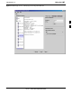
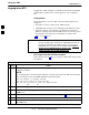
Using the LMF 68P09258A31–A Figure 3-4: BTS Login screen – identifying circuit and packet BTS files 3 Oct 2003 1X SCt 4812T BTS Optimization/ATP 3-21
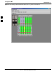
Using the LMF 68P09258A31–A Figure 3-5: Self–Managed Network Elements (NEs) state of a packet mode SC4812T 3 3-22 1X SCt 4812T BTS Optimization/ATP Oct 2003
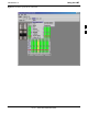
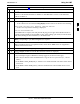
Using the LMF 68P09258A31–A Figure 3-6: Available packet mode commands 3 Oct 2003 1X SCt 4812T BTS Optimization/ATP 3-23
Using the LMF 68P09258A31–A Figure 3-7: Packet mode site with MCC–1 and BBX–1 under LMF control 3 3-24 1X SCt 4812T BTS Optimization/ATP Oct 2003
Using the LMF 68P09258A31–A Command Line Interface Overview The LMF also provides Command Line Interface (CLI) capability. Activate the CLI by clicking on a shortcut icon on the desktop. The CLI can not be launched from the GUI, only from the desktop icon. Both the GUI and the CLI use a program known as the handler. Only one handler can be running at one time. Due to architectural limitations, the GUI must be started before the CLI if you want the GUI and CLI to use the same handler.
Using the LMF 68P09258A31–A Logging into a BTS Logging into a BTS establishes a communication link between the BTS and the LMF. An LMF session can be logged into only one BTS at a time. Prerequisites Before attempting to log into a BTS, ensure the following have been completed: S The LMF is correctly installed on the LMF computer. S A bts-nnn folder with the correct CDF/NECF and CBSC files exists.
Using the LMF 68P09258A31–A Table 3-6: BTS GUI Login Procedure n Step Action NOTE 128.0.0.2 is the default IP address for MGLI–1 in field BTS units. 128.0.0.1 is the default IP address for MGLI–2. 7 Type in the correct IP Port number (normally 9216) if not correctly displayed in the IP Port box. 8 Click on Ping. – If the connection is successful, the Ping Display window shows text similar to the following: 3 Reply from 128 128.0.0.
Using the LMF 68P09258A31–A BTS Login from the CLI Environment Follow the procedure in Table 3-7 to log into a BTS when using the CLI environment. NOTE If the CLI and GUI environments are to be used at the same time, the GUI must be started first and BTS login must be performed from the GUI. Refer to Table 3-6 to start the GUI environment and log into a BTS.
Using the LMF 68P09258A31–A Logging Out Logging out of a BTS is accomplished differently for the GUI and CLI operating environments. NOTE The GUI and CLI environments use the same connection to a BTS. If a GUI and the CLI session are running for the same BTS at the same time, logging out of the BTS in either environment will log out of it for both. When either a login or logout is performed in the CLI window, there is no GUI indication that the login or logout has occurred.
Using the LMF 68P09258A31–A Logging Out of a BTS from the CLI Environment Follow the procedure in Table 3-9 to logout of a BTS when using the CLI environment. Table 3-9: BTS CLI Logout Procedure n Step Action NOTE If the BTS is also logged into from a GUI running at the same time and further work must be done with it in the GUI, proceed to Step 2. 1 3 Log out of a BTS by entering the following command: logout bts– A response similar to the following will be displayed: LMF> 13:24:51.
Using the LMF 68P09258A31–A Establishing an MMI Communication Session Equipment Connection – Figure 3-8 illustrates common equipment connections for the LMF computer. For specific connection locations on FRUs, refer to the illustration accompanying the procedures which require the MMI communication session. Initiate MMI Communication – For those procedures which require MMI communication between the LMF and BTS FRUs, follow the procedures in Table 3-10 to initiate the communication session.
Using the LMF 68P09258A31–A Figure 3-8: CDMA LMF Computer Common MMI Connections To FRU MMI port 8–PIN NULL MODEM BOARD (TRN9666A) 8–PIN TO 10–PIN RS–232 CABLE (P/N 30–09786R01) 3 LMF COMPUTER RS–232 CABLE COM1 OR COM2 DB9–TO–DB25 ADAPTER FW00687 Online Help Task oriented online help is available in the LMF by clicking on Help in the window menu bar, and selecting LMF Help from the pull–down menu.
Pinging the Processors 68P09258A31–A Pinging the Processors Pinging the BTS For proper operation, the integrity of the Ethernet LAN A and B links must be be verified. Figure 3-9 represents a typical BTS Ethernet configuration. The drawing depicts one link (of two identical links), A and B. Ping is a program that routes request packets to the LAN network modules to obtain a response from the specified “targeted” BTS.
Pinging the Processors 68P09258A31–A NOTE IMPORTANT: The Ethernet LAN A and B cables must be installed on each frame/enclosure before performing this test. All other processor board LAN connections are made via the backplanes. Table 3-11: Pinging the Processors n Step 3 Action 1 If you have not already done so, connect the LMF to the BTS (see Table 3-5 on page 3-17). 2 From the Windows desktop, click the Start button and select Run.
Download the BTS 68P09258A31–A Download the BTS Overview Before a BTS can operate, each equipped device must contain device initialization (ROM) code. ROM code is loaded in all devices during manufacture or factory repair, or, for software upgrades, from the CBSC using the DownLoad Manager (DLM). Device application (RAM) code and data must be downloaded to each equipped device by the user before the BTS can be made fully functional for the site where it is installed.
Download the BTS 68P09258A31–A When code is downloaded to an MGLI or GLI, the LMF automatically also downloads data and then enables the MGLI. When enabled, the MGLI will change to INS_ACT (bright green). A redundant GLI will not be automatically enabled and will remain OOS_RAM (yellow). When the redundant GLI is manually commanded to enable through the LMF, it will change state to INS_SBY (olive green). For non–MGLI devices, data must be downloaded after RAM code is downloaded.
Download the BTS 68P09258A31–A Verify GLI ROM Code Loads Devices should not be loaded with a RAM code version which is not compatible with the ROM code with which they are loaded. Before downloading RAM code and data to the processor cards, follow the procedure in Table 3-12 to verify the GLI devices are loaded with the correct ROM code for the software release used by the BSS.
Download the BTS 68P09258A31–A Download RAM Code and Data to MGLI and GLI Follow the procedure in Table 3-13 to download the firmware application code for the MGLI. The download code action downloads data and also enables the MGLI. Prerequisite S Prior to performing this procedure, ensure a code file exists for each of the devices to be loaded. S The LMF computer is connected to the BTS (refer to Table 3-5), and is logged in using the GUI environment (refer to Table 3-6).
Download the BTS 68P09258A31–A Download Code and Data to Non–GLI Devices Downloads to non–GLI devices can be performed individually for each device or all equipped devices can be downloaded with one action. NOTE – When downloading multiple devices, the download may fail for some of the devices (a time out occurs). These devices can be downloaded separately after completing the multiple download. – CSM devices are RAM code–loaded at the factory.
Download the BTS 68P09258A31–A Select CSM Clock Source CSMs must be enabled prior to enabling the MCCs. Procedures in the following two sub-sections cover the actions to accomplish this. For additional information on the CSM sub–system, see “Clock Synchronization Manager (CSM) Sub–system Description” in the CSM System Time – GPS & LFR/HSO Verification section of this chapter. Select CSM Clock Source A CSM can have three different clock sources.
Download the BTS 68P09258A31–A Enable CSMs NOTE – CSMs are code loaded at the factory. This data is retained in EEPROM. The download code procedure is required in the event it becomes necessary to code load CSMs with updated software versions. Use the status function to determine the current code load versions. – The CSM(s) to be enabled must have been downloaded with code (Yellow, OOS–RAM) and data. Each BTS CSM system features two CSM boards per site.
Download the BTS 68P09258A31–A Table 3-16: Enable CSMs n Step Action NOTE – If equipped with two CSMs, CSM–1 should be bright green (INS–ACT) and CSM–2 should be dark green (INS–STY) – After the CSMs have been successfully enabled, observe the PWR/ALM LEDs are steady green (alternating green/red indicates the card is in an alarm state). 3 If more than an hour has passed, refer to CSM Verification, see Figure 3-11 and Table 3-20 to determine the cause.
68P09258A31–A CSM System Time – GPS & LFR/HSO Verification CSM System Time – GPS & LFR/HSO Verification CSM & LFR Background The primary function of the Clock Synchronization Manager (CSM) boards (slots 1 and 2) is to maintain CDMA system time. The CSM in slot 1 is the primary timing source while slot 2 provides redundancy. The CSM2 card (CSM second generation) is required when using the remote GPS receiver (R–GPS). R–GPS uses a GPS receiver in the antenna head that has a digital output to the CSM2 card.
CSM System Time – GPS & LFR/HSO Verification 68P09258A31–A Low Frequency Receiver/High Stability Oscillator (LFR/HSO) The CSM and the LFR/HSO – The CSM performs the overall configuration and status monitoring functions for the LFR/HSO. In the event of GPS failure, the LFR/HSO is capable of maintaining synchronization initially established by the GPS reference signal. LFR – The LFR requires an active external antenna to receive LORAN–C RF signals.
CSM System Time – GPS & LFR/HSO Verification 68P09258A31–A CSM Frequency Verification The objective of this procedure is the initial verification of the CSM boards before performing the RF path verification tests. Parts of this procedure will be repeated for final verification after the overall optimization has been completed. Null Modem Cable A null modem cable is required. It is connected between the MMI port of the primary CSM and the null modem board.
CSM System Time – GPS & LFR/HSO Verification 68P09258A31–A Test Equipment Setup: GPS & LFR/HSO Verification Follow the procedure in Table 3-19 to set up test equipment while referring to Figure 3-11 as required. Table 3-19: Test Equipment Setup (GPS & LFR/HSO Verification) Step 1 Action Perform one of the following operations: S For local GPS (RF–GPS), verify a CSM board with a GPS receiver is installed in primary CSM slot 1 and that CSM–1 is INS.
CSM System Time – GPS & LFR/HSO Verification 68P09258A31–A Figure 3-11: CSM MMI terminal connection REFERENCE OSCILLATOR CSM board shown removed from frame MMI SERIAL PORT 3 EVEN SECOND TICK TEST POINT REFERENCE GPS RECEIVER ANTENNA INPUT ANTENNA COAX CABLE GPS RECEIVER 19.6 MHZ TEST POINT REFERENCE (NOTE 1) NULL MODEM BOARD (TRN9666A) 9–PIN TO 9–PIN RS–232 CABLE FW00372 LMF NOTEBOOK DB9–TO–DB25 ADAPTER COM1 NOTES: 1.
CSM System Time – GPS & LFR/HSO Verification 68P09258A31–A GPS Initialization/Verification Follow the procedure in Table 3-20 to initialize and verify proper GPS receiver operation. Prerequisites Ensure the following prerequisites have been met before proceeding: S The LMF is not logged into the BTS. S The COM1 port is connected to the MMI port of the primary CSM via a null modem board (see Figure 3-11). 3 S The primary CSM and HSO (if equipped) have been warmed up for at least 15 minutes.
68P09258A31–A CSM System Time – GPS & LFR/HSO Verification Table 3-20: GPS Initialization/Verification Step Action 1 To verify that Clock alarms (0000), Dpll is locked and has a reference source, and GPS self test passed messages are displayed within the report, issue the following MMI command bstatus – Observe the following typical response: Clock Alarms (0000): DPLL is locked and has a reference source.
CSM System Time – GPS & LFR/HSO Verification 68P09258A31–A Table 3-20: GPS Initialization/Verification Step 3 Action 4 If any of the above mentioned areas fail, verify: – If LED is RED, verify that HSO had been powered up for at least 5 minutes.
68P09258A31–A CSM System Time – GPS & LFR/HSO Verification Table 3-20: GPS Initialization/Verification Step Action 7 Verify the following GPS information (shown above in underlined text): – At least 4 satellites are tracked, and 4 satellites are visible. – GPS Receiver Control Task State is “tracking satellites”. Do not continue until this occurs! – Dilution of Precision indication is not more that 30.
CSM System Time – GPS & LFR/HSO Verification 68P09258A31–A Table 3-20: GPS Initialization/Verification Step 10 Action Observe the following typical response if the CSM is warmed up.
CSM System Time – GPS & LFR/HSO Verification 68P09258A31–A Table 3-21: LFR Initialization/Verification Step Action 1 At the CSM> prompt, enter lstatus to verify that the LFR is in tracking mode.
CSM System Time – GPS & LFR/HSO Verification 68P09258A31–A Table 3-21: LFR Initialization/Verification Step 4 Action Note LORAN–C LFR information (highlighted above in boldface type) is usually the #1 reference source (verified from left to right). NOTE If any of the above mentioned areas fail, verify: – The LFR antenna is not obstructed or misaligned. – The antenna pre–amplifier power and calibration twisted pair connections are intact and < 91.4 m (300 ft) in length.
68P09258A31–A CSM System Time – GPS & LFR/HSO Verification Prerequisites S The LMF is not logged into the BTS. S The COM1 port is connected to the MMI port of the primary CSM via a null modem board. S The primary CSM and the HSO (if equipped) have warmed up for 15 minutes. If the BTS is equipped with an HSO, follow the procedure in Table 3-22 to configure the HSO. Table 3-22: HSO Initialization/Verification Step 1 3 Action At the BTS, slide the HSO card into the cage.
Test Equipment Set-up 68P09258A31–A Test Equipment Set-up Connecting Test Equipment to the BTS The following equipment is required to perform optimization: S S S S S S 3 LMF Test set Directional coupler and attenuator RF cables and connectors Null modem cable (see Figure 3-10) GPIB interface box Refer to Table 3-23 and Table 3-24 for an overview of connections for test equipment currently supported by the LMF.
Test Equipment Set-up 68P09258A31–A Supported Test Equipment CAUTION To prevent damage to the test equipment, all TX test connections must be through the directional coupler and in-line attenuator as shown in the test setup illustrations.
Test Equipment Set-up 68P09258A31–A Test Equipment Connection Charts To use the following charts to identify necessary test equipment connections, locate the communications system analyzer being used in the COMMUNICATIONS SYSTEM ANALYZER columns, and read down the column. Where a dot appears in the column, connect one end of the test cable to that connector. Follow the horizontal line to locate the end connection(s), reading up the column to identify the appropriate equipment and/or BTS connector.
Test Equipment Set-up 68P09258A31–A CDMA2000 1X/IS–95A/B–capable Test Equipment Connections Table 3-24 depicts the interconnection requirements for currently available test equipment supporting both CDMA 2000 1X and IS–95A/B which meets Motorola standards and is supported by the LMF. Table 3-24: CDMA2000 1X/IS–95A/B Test Equipment Interconnection COMMUNICATIONS SYSTEM ANALYZER SIGNAL EVEN SECOND SYNCHRONIZATION 19.
Test Equipment Set-up 68P09258A31–A Equipment Warm-up 3 NOTE To assure BTS stability and contribute to optimization accuracy of the BTS, warm-up the BTS test equipment prior to performing the BTS optimization procedure as follows: – Agilent E7495A for a minimum of 30 minutes – All other test sets for a minimum of 60 minutes Time spent running initial or normal power-up, hardware/ firmware audit, and BTS download counts as warm-up time.
Test Equipment Set-up 68P09258A31–A Figure 3-12: IS–95A/B Cable Calibration Test Setup – CyberTest, Agilent 8935, Advantest R3465, and HP 8921A SUPPORTED TEST SETS CALIBRATION SET UP Motorola CyberTest A. SHORT CABLE CAL ÎÎÎ ÎÎÎÏ SHORT CABLE TEST SET 3 ANT IN RF GEN OUT Note: The Directional Coupler is not used with the Cybertest Test Set. The TX cable is connected directly to the Cybertest Test Set. B.
Test Equipment Set-up 68P09258A31–A Figure 3-13: IS–95A/B and CDMA 2000 1X Cable Calibration Test Setup – Agilent E4406A/E4432B and Advantest R3267/R3562 SUPPORTED TEST SETS CALIBRATION SET UP A. SHORT CABLE CAL Agilent E4432B (Top) and E4406A (Bottom) SHORT CABLE TEST SET RF OUTPUT 50 OHM 3 B. RX TEST SETUP RF INPUT 50 OHM N–N FEMALE ADAPTER Advantest R3267 (Top) and R3562 (Bottom) RX CABLE SHORT CABLE TEST SET RF IN EXT TRIG IN MOD TIME BASE IN (EXT REF IN) RF OUT C.
Test Equipment Set-up 68P09258A31–A Figure 3-14: CDMA2000 1X Cable Calibration Test Setup – Agilent 8935/E4432B CALIBRATION SET UP SUPPORTED TEST SETS A. SHORT CABLE CAL Agilent E4432B (Top) and 8935 Series E6380A (Bottom) SHORT CABLE TEST SET 3 ÁÁ Á ÁÁÁ RF OUTPUT 50 Ω B. RX TEST SETUP N–N FEMALE ADAPTER RX CABLE ANT IN SHORT CABLE NOTE: TEST SET 10 MHZ IN ON REAR OF SIGNAL GENERATOR IS CONNECTED TO 10 MHZ REF OUT ON SIDE OF CDMA BASE STATION TEST SET. D. TX TEST SETUP 50 Ω ΤERM.
Test Equipment Set-up 68P09258A31–A Figure 3-15: CDMA2000 1X Cable Calibration Test Setup – Agilent E7495A SUPPORTED TEST SETS Agilent E7495A CALIBRATION SET UP A. SHORT CABLE CAL 10 DB PAD SHORT CABLE TEST SET 10 DB PAD 3 D. RX and TX TEST SETUP 50 Ω ΤERM.
Test Equipment Set-up 68P09258A31–A Set-up for TX Calibration Figure 3-16 through Figure 3-18 show the test set connections for TX calibration. Figure 3-16: TX Calibration Test Setup – CyberTest (IS–95A/B) and Agilent 8935 (IS–95A/B and CDMA2000 1X), and Advantest R3465 TEST SETS TRANSMIT (TX) SET UP Motorola CyberTest POWER SENSOR 100–WATT (MIN) NON–RADIATING RF LOAD ÎÎÎÎ ÎÎÎÎÏ FRONT PANEL 3 OUT 2O DB PAD (FOR 1.7/1.9 GHZ) NOTE: THE DIRECTIONAL COUPLER IS NOT USED WITH THE CYBERTEST TEST SET.
Test Equipment Set-up 68P09258A31–A Figure 3-17: TX Calibration Test Setup – Agilent E4406A and Advantest R3567 (IS–95A/B and CDMA2000 1X) TEST SETS TRANSMIT (TX) SET UP Advantest Model R3267 POWER SENSOR 100–WATT (MIN) NON–RADIATING RF LOAD POWER METER (OPTIONAL)* OUT 3 2O DB PAD (FOR 1.7/1.
Test Equipment Set-up 68P09258A31–A Figure 3-18: TX Calibration Test Setup – Agilent E7495A (IS–95A/B and CDMA2000 1X) TEST SETS TRANSMIT (TX) SET UP Agilent E7495A POWER SENSOR NOTE: IF BTS IS EQUIPPED WITH DUPLEXED RX/TX SIGNALS, CONNECT THE TX TEST CABLE TO THE DUPLEXED ANTENNA CONNECTOR. POWER METER PORT 1 RF OUT COMMUNICATIONS SYSTEM ANALYZER 100–WATT (MIN.) NON–RADIATING RF LOAD PORT 2 RF IN INTERNAL ETHERNET CARD TX TEST CABLE 3 DIRECTIONAL COUPLER (30 DB) 50 Ω TERM .
Test Equipment Set-up 68P09258A31–A Setup for Optimization/ATP Figure 3-19 and Figure 3-21 show test set connections for IS–95 A/B optimization/ATP tests. Figure 3-21 and Figure 3-22 show test set connections for IS-95 A/B/C optimization/ATP tests. Figure 3-19: Optimization/ATP Test Setup Calibration – Agilent 8935 TEST SET Optimization/ATP SET UP Agilent 8935 Series E6380A (formerly HP 8935) 3 SYNC MONITOR EVEN SEC TICK PULSE REFERENCE FROM CSM BOARD FREQ MONITOR 19.
Test Equipment Set-up 68P09258A31–A Figure 3-20: Optimization/ATP Test Setup – HP 8921 TEST SETS Optimization/ATP SET UP Hewlett–Packard Model HP 8921A W/PCS Interface (for 1700 and 1900 MHz) SYNC MONITOR EVEN SEC TICK PULSE REFERENCE FROM CSM BOARD FREQ MONITOR 19.6608 MHZ CLOCK REFERENCE FROM CSM BOARD NOTE: IF BTS RX/TX SIGNALS ARE DUPLEXED (4800E): BOTH THE TX AND RX TEST CABLES CONNECT TO THE DUPLEXED ANTENNA GROUP.
Test Equipment Set-up 68P09258A31–A Figure 3-21: IS–95A/B and CDMA2000 1X Optimization/ATP Test Setup – Advantest R3267/3562, Agilent E4432B/E4406A TEST SETS Optimization/ATP SET UP Advantest R3267 (Top) and R3562 (Bottom) TO EXT TRIG ON REAR OF SPECTRUM ANALYZER 10 MHZ REF OUT NOTE: IF BTS RX/TX SIGNALS ARE DUPLEXED: BOTH THE TX AND RX TEST CABLES CONNECT TO THE DUPLEXED ANTENNA GROUP. BASEBAND GEN. REF.
Test Equipment Set-up 68P09258A31–A Figure 3-22: IS–95A/B and CDMA2000 1X Optimization/ATP Test Setup – Agilent E7495A ATP TEST SET UP TEST SET POWER METER Agilent E7495A NOTE: IF BTS IS EQUIPPED WITH DUPLEXED RX/TX SIGNALS, CONNECT THE TX TEST CABLE TO THE DUPLEXED ANTENNA CONNECTOR. RX TEST RF INPUT 50 Ω OR INPUT 50 Ω 100–WATT (MIN.
Test Equipment Set-up 68P09258A31–A ATP Setup with Directional Couplers Figure 3-23 shows a typical TX ATP setup.
Test Equipment Set-up 68P09258A31–A Figure 3-24: Typical RX ATP Setup with Directional Coupler Figure 3-24 shows a typical RX ATP setup. COBRA RFDS Detail RX ANTENNA DIRECTIONAL COUPLERS RX RF FROM BTS FRAME 2 3 4 5 6 RX (RFM TX) 1 TX (RFM RX) RFDS TX (RFM RX) COUPLER OUTPUTS TO RFDS FWD(BTS) ASU1 (SHADED) CONNECTORS 3 RF FEED LINE TO TX ANTENNA REMOVED Connect RX test cable between the test set and the appropriate RX antenna directional coupler.
Test Set Calibration 68P09258A31–A Test Set Calibration Background Proper test equipment calibration ensures that the test equipment and associated test cables do not introduce measurement errors, and that measurements are correct. NOTE If the test equipment set being used to optimize or test the BTS has been calibrated and maintained as a set, this procedure does not need to be performed. This procedure must be performed prior to beginning the optimization.
Test Set Calibration 68P09258A31–A Cable Calibration – Manual cable calibration procedures using the HP 8921A and Advantest R3465 communications system analyzers are provided in the Manual Cable Calibration section of Appendix F, if needed. GPIB Addresses GPIB addresses can range from 1 through 30. The LMF will accept any address in that range, but the numbers entered in the LMF Options window GPIB address box must match the addresses of the test equipment.
Test Set Calibration 68P09258A31–A Manually Selecting Test Equipment in a Serial Connection Tab Test equipment can be manually specified before, or after, the test equipment is connected. The LMF does not check to see if the test equipment is actually detected for manual specification. Follow the procedure in Table 3-25 to select test equipment manually.
Test Set Calibration 68P09258A31–A Automatically Selecting Test Equipment in Serial Connection Tab When using the auto-detection feature to select test equipment, the LMF examines which test equipment items are actually communicating with the LMF. Follow the procedure in Table 3-26 to use the auto-detection feature. Table 3-26: Selecting Test Equipment Using Auto-Detect n Step Action 1 In the LMF window menu bar, click Tools and select Options... from the pull–down menu. The LMF Options window appears.
Test Set Calibration 68P09258A31–A Calibrating Test Equipment The calibrate test equipment function zeros the power measurement level of the test equipment item that is to be used for TX calibration and audit. If both a power meter and an analyzer are connected, only the power meter is zeroed. NOTE The Agilent E4406A transmitter tester does not support power measurement level zeroing. Refer to the Equipment Calibration section of Appendix F for E4406A calibration.
Test Set Calibration 68P09258A31–A Calibrating Cables Overview The LMF Cable Calibration function is used to measure the path loss (in dB) for the TX and RX cables, adapters, directional couplers, and attenuators that make up the cable configurations used for testing. A communications system analyzer is used to measure the loss of both the TX test cable and the RX test cable configurations.
Test Set Calibration 68P09258A31–A Calibrate Test Cabling using Communications System Analyzer Cable Calibration is used to calibrate both TX and RX test cables. Appendix F covers the procedures for manual cable calibration. NOTE 3 LMF cable calibration cannot be accomplished using an HP8921 analyzer for 1.7/1.9 GHz. A different analyzer type or the signal generator and spectrum analyzer method (Table 3-29 and Figure 3-25) must be used.
Test Set Calibration 68P09258A31–A Calibrate Test Cabling Using Signal Generator & Spectrum Analyzer Follow the procedure in Table 3-29 to calibrate the TX/Duplexed RX cables using a signal generator and spectrum analyzer. Refer to Figure 3-25, if required. Follow the procedure in Table 3-30 to calibrate the Non–Duplexed RX cables using the signal generator and spectrum analyzer. Refer to Figure 3-26, if required.
Test Set Calibration 68P09258A31–A Table 3-30: Calibrating Non–Duplexed RX Cables Using a Signal Generator &Spectrum Analyzer Step Action NOTE When preparing to calibrate a BTS with Duplexed TX and RX the RX cable calibration must be done using calibration setup in Figure 3-25 and the procedure in Table 3-29. 3 1 Connect a short test cable between the spectrum analyzer and the signal generator as shown in Figure 3-26, detail “A” (top portion of figure).
Test Set Calibration 68P09258A31–A Setting Cable Loss Values Cable loss values for TX and RX test cable configurations are normally set by accomplishing automatic cable calibration using the LMF and the applicable test equipment. The LMF stores the measured loss values in the cable loss files. The cable loss values can also be set or changed manually. Follow the procedure in Table 3-31 to set cable loss values.
Test Set Calibration 68P09258A31–A Setting TX Coupler Loss Values If an in–service TX coupler is installed, the coupler loss (e.g., 30 dB) must be manually entered so it will be included in the LMF TX calibration and audit calculations and RX FER Test. Follow the procedure in Table 3-32 to set coupler loss values.
Bay Level Offset Calibration 68P09258A31–A Bay Level Offset Calibration Introduction Bay Level Offset (BLO) calibration is the central activity of the optimization process. BLO calibration compensates for normal equipment variations within the BTS RF paths and assures the correct transmit power is available at the BTS antenna connectors to meet site performance requirements.
Bay Level Offset Calibration 68P09258A31–A TX Path Calibration The TX Path Calibration assures correct site installation, cabling, and the first order functionality of all installed equipment. The proper function of each RF path is verified during calibration. The external test equipment is used to validate/calibrate the TX paths of the BTS. WARNING Before installing any test equipment directly to any TX OUT connector you must first verify that there are no CDMA channels keyed.
Bay Level Offset Calibration 68P09258A31–A S The calibration data for a BBX is organized as a large flat array. The array is organized by branch, sector, and calibration point. – The first breakdown of the array indicates which branch the contained calibration points are for. The array covers transmit, main receive and diversity receive offsets as follows: Table 3-33: BLO BTS.
Bay Level Offset Calibration 68P09258A31–A Table 3-34: BTS.
Bay Level Offset Calibration 68P09258A31–A Test Equipment Set-up for RF Path Calibration Follow the procedure in Table 3-35 to set up test equipment. Table 3-35: Set Up Test Equipment for RF Path Calibration Step Action 1 If it has not already been done, refer to the procedure in Table 3-5 (on page 3-17) to interface the LMF computer terminal to the frame LAN A connector. 2 If it has not already been done, refer to Table 3-6 (on page 3-26) to start a GUI LMF session.
Bay Level Offset Calibration 68P09258A31–A TX Calibration and the LMF The LMF Tests > TX > TX Calibration... and Tests > All Cal/Audit... selections perform TX BLO calibration testing for installed BBX(s). The All Cal/Audit... selection initiates a series of actions to perform TX calibration, and if calibration is successful, download BLO and perform TX audit. The TX Calibration... selection performs only TX calibration. When TX Calibration...
Bay Level Offset Calibration 68P09258A31–A Test Pattern Drop-down Pick List The Tests > TX > TX Calibration... menu window has a Test Pattern pull–down menu. This menu has the following choices: S Pilot (default) – performs tests using a pilot signal only. This pattern should be used when running in–service tests. It only requires a BBX to do the test. S Standard – performs the tests using pilot, synch, paging and six traffic channels. This pattern should be used on all non–in–service tests.
Bay Level Offset Calibration 68P09258A31–A TX Calibration 3 WARNING Before installing any test equipment directly to any TX OUT connector, first verify there are no CDMA BBX channels keyed. Failure to do so can result in serious personal injury and/or equipment damage. CAUTION Always wear an approved anti–static wrist strap while handling any circuit card or module. If this is not done, there is a high probability that the card or module could be damaged by ESD.
Bay Level Offset Calibration 68P09258A31–A Table 3-37: All Cal/Audit and TX Calibration Procedure n Step Action 4 For All Cal Audit... – Click Tests in the BTS menu bar, and select TX > All Cal/Audit... from the pull–down menus. A CDMA Test Parameters window will appear. For TX Calibration – Click Tests in the BTS menu bar, and select TX > TX Calibration from the pull–down menus. A CDMA Test Parameters window will appear.
Bay Level Offset Calibration 68P09258A31–A Download BLO Procedure After a successful TX path calibration, download the bay level offset (BLO) calibration file data to the BBXs. BLO data is extracted from the CAL file for the Base Transceiver Subsystem (BTS) and downloaded to the selected BBX devices. If a successful All Cal/Audit was completed, this procedure does not need to be performed, as BLO is downloaded as part of the All Cal/Audit.
Bay Level Offset Calibration 68P09258A31–A TX Path Audit Perform the calibration audit of the TX paths of all equipped BBX slots per the procedure in Table 3-39 WARNING Before installing any test equipment directly to any TX OUT connector, first verify there are no CDMA BBX channels keyed. Failure to do so can result in serious personal injury and/or equipment damage.
Bay Level Offset Calibration 68P09258A31–A TX Path Audit procedure After a TX calibration has been performed, or if verification of BLO data in the CAL file is required, follow the procedure in Table 3-39 to perform a BTS TX path audit. Table 3-39: BTS TX Path Audit n Step 1 2 3 3 4 5 Action If it has not already been done, configure test equipment for TX path audit by following the procedure in Table 3-35 (TX audit uses the same configuration as TX calibration). Select the BBX(s) to be audited.
Bay Level Offset Calibration 68P09258A31–A All Cal/Audit Test The Tests menu item, All Cal/Audit, performs the TX BLO Calibration and Audit test for a XCVR(s). All measurements are made through the appropriate TX output connector using the calibrated TX cable setup. NOTE If the TX calibration portion of the test passes, the BLO data is automatically downloaded to the BBX(s) before the audit portion of the test is run.
Bay Level Offset Calibration 68P09258A31–A Table 3-40: All Cal/Audit Test n Step 9 10 Action Follow the cable connection directions as they are displayed. A status report window displays the test results. Click on Save Results or Dismiss to close the status report window. Create CAL File The Create Cal File function gets the BLO data from BBXs and creates/updates the CAL file for the BTS. If a CAL file does not exist, a new one is created. If a CAL file already exists, it is updated.
RFDS Set–up and Calibration 68P09258A31–A RFDS Set–up and Calibration RFDS Description NOTE The RFDS is not available for the –48 V BTS at the time of this publication. The optional RFDS performs RF tests of the site from the CBSC or from an LMF.
RFDS Set–up and Calibration 68P09258A31–A Checking and Setting RFDS Parameters Follow the procedure in Table 3-42 to review and/or edit RFDS parameters. Table 3-42: RFDS Parameter Settings Step 3 Action 1 Important! Log out of the BTS prior to performing this procedure. 2 Using a text editor, verify the following fields are set correctly in the bts–#.
RFDS Set–up and Calibration 68P09258A31–A Table 3-42: RFDS Parameter Settings Step Action – Click on Device in the BTS menu bar, and select Enable from the pull–down menu. A status report window shows the status of the operation. – When the operation is complete, click OK to close the status report window. 6i 6jj ! CAUTION When the MGLI changes to INS_ACT, data will automatically be downloaded to the RFDS.
RFDS Set–up and Calibration 68P09258A31–A RFDS TSU NAM Programming The Number Assignment Module (NAM) information needs to be programmed into the TSU before it can receive and process test calls, or be used for any type of RFDS test. The RFDS TSU NAM must be programmed with the appropriate system parameters and phone number during hardware installation. The TSU phone and TSU MSI must be recorded for each BTS used for OMC–R RFDS software configuration.
RFDS Set–up and Calibration 68P09258A31–A Valid NAM Ranges Table 3-44 provides the valid NAM field ranges. If any of the fields are missing or out of range, the RFDS errors out.
RFDS Set–up and Calibration 68P09258A31–A Set Antenna Map Data The antenna map data must be entered manually if an RFDS is installed. Antenna map data does not need to be entered if an RFDS is not installed. The antenna map data is only used for RFDS tests and is required if an RFDS is installed. Prerequisite S Logged into the BTS Follow the procedure in Table 3-45 to set antenna map data for the RFDS.
RFDS Set–up and Calibration 68P09258A31–A Set RFDS Configuration Data If an RFDS is installed, the RFDS configuration data must be manually entered. Prerequisite S LMF is logged into the BTS The entered antenna# index numbers must correspond to the antenna# index numbers used in the antenna maps. NOTE Follow the procedure in Table 3-46 to set the RFDS Configuration Data. Table 3-46: Set RFDS Configuration Data Step Action 1 Click on Util in the BTS menu bar, and select Edit > RFDS Configuration...
RFDS Set–up and Calibration 68P09258A31–A RFDS Calibration The RFDS Calibration option is used to calibrate the RFDS TX and RX paths. TX Path Calibration – For a TX antenna path calibration the BTS XCVR is keyed at a pre–determined power level and the BTS power output level is measured by the RFDS. The power level is then measured at the TX antenna directional coupler by the power measuring test equipment item being used (power meter or analyzer).
RFDS Set–up and Calibration 68P09258A31–A RFDS Calibration Procedure Follow the procedure in Table 3-48 to perform RFDS calibration. Table 3-48: RFDS Calibration Procedure Step Action 1 In the LMF, select the CDMA BTS–xxx tab. 2 If the BTS Control button is not selected (no black dot showing), click on the B button in the BTS menu bar to select it.
RFDS Set–up and Calibration 68P09258A31–A Program TSU NAM The NAM must be programmed before it can receive and process test calls, or be used for any type of RFDS test. Prerequisites Ensure the following prerequisites have been met before proceeding: S MGLI is INS. S TSU is powered up and has a code load. 3 Program NAM Procedure Follow the procedure in Table 3-49 to program the TSU NAM. Table 3-49: Program the TSU NAM Step Action 1 Select the RFDS tab.
BTS Redundancy/Alarm Testing 68P09258A31–A BTS Redundancy/Alarm Testing Objective This section tests the redundancy options that could be included in the cell site. These tests verify, under a fault condition, that all modules equipped with redundancy switch operations to their redundant partner and resume operation. An example would be to pull the currently active CSM and verify the standby CSM takes over distribution of the CDMA reference signal. Redundancy covers many BTS modules.
BTS Redundancy/Alarm Testing 68P09258A31–A Test Equipment Setup Follow the procedure in Table 3-50 to set up test equipment: NOTE All alarm tests are performed using TX antenna 1 Table 3-50: Test Equipment Setup for Redundancy/Alarm Tests 3 Step Action 1 Interface the LMF computer to the BTS LAN A connector on the BTS frame (refer to Table 3-5, page 3-17). 2 Login to the BTS. 3 Set up test equipment for TX Calibration at TXOUT1 (see Figure 3-16).
BTS Redundancy/Alarm Testing 68P09258A31–A Power Supply Redundancy Follow the steps in Table 3-51 to verify redundancy of the power supply modules. Alarms reported by the master GLI (displayed via the alarm monitor) are also verified.
BTS Redundancy/Alarm Testing 68P09258A31–A MPC/EMPC–1 ÂÂÂÂÂÂ ÂÂÂÂÂÂ ÂÂÂÂÂÂ ÂÂÂÂÂÂ Á Á Á Á MPC/EMPC–2 Switch BBX–12 BBX–11 BBX–10 BBX–9 BBX–8 BBX–7 MCC–12 MCC–11 MCC–10 MCC–9 MCC–8 MCC–7 GLI2–2 AMR–2 38 mm Filler Panel CCD–2 CSM–2 CCD–1 CIO BBX–6 BBX–R BBX–5 BBX–4 BBX–3 BBX–2 BBX2–1 MCC–6 MCC–5 MCC–4 MCC–3 MCC–2 GLI2–1 MCC–1 AMR–1 PS–3 PS–2 PS–1 CSM–1 HSO/LFR NOTE: MCCs may be MCC8Es, MCC24s, or MCC–1Xs. BBXs may be BBX2s or BBX–1Xs. GLIs may be GLI2s or GLI3s.
BTS Redundancy/Alarm Testing 68P09258A31–A Miscellaneous Alarm/Redundancy Tests Follow the steps in Table 3-52 to verify alarms reported by the master GLI are displayed via the alarm monitor if a BTS frame module failure occurs. Table 3-52: Miscellaneous Alarm Tests Step 1 2 Action Select Util>Alarm Monitor to display the alarm monitor window. Perform the following to verify fan module alarms: • Unseat a fan module (see Figure 3-29 or Figure 3-30).
BTS Redundancy/Alarm Testing 68P09258A31–A Figure 3-29: +27 V BTS C-CCP Fan Modules LATCHES FAN MODULE FAN MODULE REAR REAR FRONT PWR/ALM FAN MODULE REAR PWR/ALM FRONT FRONT PWR/ALM 3 FAN MODULES FW00130 Figure 3-30: –48 V BTS C-CCP and Power Conversion Shelf Fan Modules LATCHES FAN MODULE REAR FRONT FAN MODULE REAR PWR/ALM FRONT FAN MODULE REAR PWR/ALM FRONT PWR/ALM FAN MODULES LATCHES FAN MODULE REAR FRONT FAN MODULE REAR PWR/ALM FRONT PWR/ALM FW00489 FAN MODULES BBX Re
BTS Redundancy/Alarm Testing 68P09258A31–A Table 3-53: BBX Redundancy Alarms Step Action n WARNING Any BBXs enabled will immediately key-up. Before enabling any BBX, always verify that the TX output assigned to the BBX is terminated into a 50 W non-radiating RF load! Failure to do so could result in serious personal injury and/or damage to the equipment. 1 Enable the primary, then the redundant BBX assigned to ANT 1 by selecting the BBX and Device>BBX/MAWI>Key.
BTS Redundancy/Alarm Testing 68P09258A31–A CSM, GPS, & LFR/HSO Redundancy/Alarm Tests Follow the procedure in Table 3-54 to verify the manual redundancy of the CSM, GPS, and LFR/HSO boards. Verification of alarms reported is also covered. NOTE DO NOT perform the procedure in Table 3-54, unless the site is configured with a LORAN–C or HSO timebase as a backup for the GPS. Table 3-54: CSM, GPS, & LFR/HSO, Redundancy/Alarm Tests 3 Step Action n WARNING Any BBXs enabled will immediately key-up.
BTS Redundancy/Alarm Testing 68P09258A31–A Table 3-54: CSM, GPS, & LFR/HSO, Redundancy/Alarm Tests Step Action * IMPORTANT DO NOT ENABLE the redundant CSM. 11 Disable CSM 2 and enable CSM 1. S Various CSM Source and Clock alarms are reported and the site comes down. S Alarms clear when the site comes back up. 12 De-key the Xcvr by selecting Device>BBX/MAWI>Dekey. 13 Allow the CSM 1 board to go INS_ACT. 3 S Verify the BBXs are de-keyed and OOS.
BTS Redundancy/Alarm Testing 68P09258A31–A Power Amplifier (PA) Redundancy Test Follow the procedure in Table 3-55 to verify redundancy of the Power Amplifiers (PA). WARNING 3 First verify there are no BBX channels keyed BEFORE moving the antenna connection. Failure to do so can result in serious personal injury and/or equipment damage.
BTS Redundancy/Alarm Testing 68P09258A31–A MGLI/GLI Redundancy Test CAUTION This test can only be performed when the MM path is established by the MM (not just with LAPD link connected). Attempting to force the GLIs to “hot swap” under alarm monitor control, when isolated from the MM, causes MGLIs to hang up.
Alarms Testing 68P09258A31–A Alarms Testing Alarm Verification ALARM connectors provide Customer Defined Alarm Inputs and Outputs. The customer can connect BTS site alarm input sensors and output devices to the BTS, thus providing alarm reporting of active sensors as well controlling output devices. The SC 4812T is capable of concurrently monitoring 36 input signals coming into the BTS.
Alarms Testing 68P09258A31–A Figure 3-31: Alarm Connector Location and Connector Pin Numbering 1 1 ÂÂÂÂÂÂÂ ÂÂÂÂÂÂÂ ÂÂÂÂÂÂÂ ÂÂÂÂÂÂÂ ÂÂÂÂÂÂÂ 2 2 59 59 60 60 3 ti-CDMA-WP-00041-v01-ildoc-ftw Purpose The following procedures verify the customer defined alarms and relay contacts are functioning properly. These tests are performed on all AMR alarms/relays in a sequential manner until all have been verified. Perform these procedures periodically to ensure the external alarms are reported properly.
Alarms Testing 68P09258A31–A Figure 3-32: AMR Connector Pin Numbering A CDI 18 ... A CDI 1 Returns 60 26 2 60 26 59 25 1 59 25 ALARM A (AMR 1) Returns 2 1 ALARM B (AMR 2) B CDI 36 ... B CDI 19 FW00302 3 NOTE The preferred method to verify alarms is to follow the Alarms Test Box Procedure, Table 3-57. If not using an Alarm Test Box, follow the procedure listed in Table 3-58.
Alarms Testing 68P09258A31–A Table 3-57: CDI Alarm Input Verification Using the Alarms Test Box Step Action 14 Set all switches on the alarms test box to the Open position. A clear alarm should be reported for each switch setting. 15 Disconnect the alarms test box from the ALARM B connector. 16 Select the MGLI. 17 Click on the Device menu. 18 Click on the Set Alarm Relays menu item. 19 Click on Normally Closed. A status report window displays the results of the action.
Alarms Testing 68P09258A31–A Table 3-57: CDI Alarm Input Verification Using the Alarms Test Box Step 3 Action 37 Disconnect the alarms test box from the ALARM A connector. 38 Connect the alarms test box to the ALARM B connector. 39 Set all switches on the alarms test box to both the Open and the Closed position. No alarm should be reported for any switch settings. 40 Disconnect the alarms test box from the ALARM B connector.
Alarms Testing 68P09258A31–A Table 3-58: CDI Alarm Input Verification Without the Alarms Test Box Step Action 12 Click on Normally Closed. A status report window displays the results of the action. 13 Click on OK to close the status report window. Alarms should be reported for alarm inputs 1 through 36. 14 Refer to Figure 3-32 and sequentially short the ALARM A connector CDI 1 through CDI 18 pins (25–26 through 59–60) together.
Alarms Testing 68P09258A31–A Pin and Signal Information for Alarm Connectors Table 3-59 lists the pins and signal names for Alarms A and B.
Chapter 4 4 Automated Acceptance Test Procedure Oct 2003 1X SCt 4812T BTS Optimization/ATP 4-1
Automated Acceptance Test Procedures 68P09258A31–A Automated Acceptance Test Procedures Introduction The Automated Acceptance Test Procedure (ATP) allows Cellular Field Engineers (CFEs) to run automated acceptance tests on all equipped BTS subsystem devices using the Local Maintenance Facility (LMF) and supported test equipment per the current Cell Site Data File (CDF) assignment. The results of these tests (at the option of the operator) are written to a file that can be printed.
Automated Acceptance Test Procedures 68P09258A31–A Reduced ATP NOTE Equipment has been factory–tested for FCC compliance. If license–governing bodies require documentation supporting SITE compliance with regulations, a full ATP may be necessary. Perform the Reduced ATP only if reports for the specific BTS site are NOT required. After downloading the proper operational software to the BTS, the CFE must perform these procedures (minimal recommendation): 1.
Automated Acceptance Test Procedures 68P09258A31–A ATP Test Options There are three different ATP testing options that can be performed to completely test a BTS. Depending on your requirements, one of the following ATP testing options should be run. Table 4-1 provides the procedure to execute an ATP test.
Automated Acceptance Test Procedures 68P09258A31–A ATP Test Prerequisites Before attempting to run any ATP tests, ensure the following have been completed: S BTS has been optimized and calibrated (see Chapter 3). S LMF is logged into the BTS. S CSMs, GLIs, BBXs, MCCs, and TSU (if the RFDS is installed) have correct code load and data load. S S S S S S Primary CSM, GLI, and MCCs are INS_ACT (bright green). BBXs are calibrated and BLOs are downloaded. No BBXs are keyed (transmitting).
Automated Acceptance Test Procedures 68P09258A31–A Required Test Equipment The following test equipment is required: S S S S WARNING 4 NOTE 4-6 LMF Power meter (used with HP8921A/600 and Advantest R3465) Communications system analyzer Signal generator for FER testing (required for all communications system analyzers for 1X FER) – Before installing any test equipment directly to any BTS TX OUT connector, verify that there are no CDMA channels keyed.
Automated Acceptance Test Procedures 68P09258A31–A Individual Acceptance Tests The following individual ATP tests can be used to evaluate specific aspects of BTS operation against individual performance requirements. All testing is performed using the LMF GUI environment. TX Testing TX tests verify any given transmit antenna path and output power control. All tests are performed using the external, calibrated test equipment. All measurements are made at the appropriate BTS TX OUT connector(s).
Automated Acceptance Test Procedures 68P09258A31–A Frame Error Rate The Frame Error Rate (FER) test verifies RX operation of the entire CDMA Reverse Link using all equipped MCCs assigned to all respective sectors/antennas. This test verifies the BTS sensitivity on all traffic channel elements currently configured on all equipped MCCs at an RF input level of –119 dBm (or –116 dBm if using TMPC).
Automated Acceptance Test Procedures 68P09258A31–A ATP Test Procedure Follow the procedure in Table 4-1 to perform any ATP test. Table 4-1: ATP Test Procedure Step 1 Action Be sure that all prerequisites described on page 4-5 have been met. NOTE If the LMF has been logged into the BTS with a different Multi–Channel Preselector setting than the one to be used for this test, the LMF must be logged out of the BTS and logged in again with the new Multi–Channel Preselector setting.
Automated Acceptance Test Procedures 68P09258A31–A Table 4-1: ATP Test Procedure Step 10 Action If applicable, select a test pattern from the Test Pattern pick list. NOTE S Selecting Pilot (default) performs tests using only a pilot signal. S Selecting Standard performs tests using pilot, synch, paging and 6 traffic channels. This requires an MCC to be selected. S Selecting CDFPilot performs tests using only a pilot signal, however, the gain for the channel elements is specified in the CDF file.
Individual ATP Test Background Information 68P09258A31–A Individual ATP Test Background Information TX Spectral Purity Transmit Mask Acceptance Test (Tx Mask) This test verifies the spectral purity of each BBX carrier keyed up at a specific frequency, per the current CDF file assignment. All tests are performed using the external calibrated test set, controlled by the same command. All measurements are via the appropriate TX OUT (BTS/RFDS) connector.
Individual ATP Test Background Information 68P09258A31–A Figure 4-1: TX Mask Verification Spectrum Analyzer Display Mean CDMA Bandwidth Power Reference .
Individual ATP Test Background Information 68P09258A31–A TX Pilot Time Offset Acceptance Test This test verifies the transmitted Pilot channel element Pilot Time Offset of each BBX carrier keyed up at a specific frequency per the current CDF file assignment. All tests are performed using the external calibrated test set controlled by the same command. All measurements are via the appropriate TX OUT (BTS/RFDS) connector.
Individual ATP Test Background Information 68P09258A31–A The BBX then de-keys and, if selected, the MCC is re-configured to assign the applicable redundant BBX to the current TX antenna path under test. The test is then repeated. Upon completion of the test, the OCNS is disabled on the specified MCC/CE. See Table 4-1 to perform this test. Figure 4-2: Code Domain Power and Noise Floor Levels Pilot Channel PILOT LEVEL MAX OCNS CHANNEL 8.2 dB 12.2 dB MAX OCNS SPEC. Active channels MIN OCNS SPEC.
68P09258A31–A Individual ATP Test Background Information up, using only bbxlvl level offsets, to generate a CDMA carrier (with pilot channel element only). BBX power output is set to –20 dBm as measured at the TX OUT connector (on either the BTS or RFDS directional coupler). The BBX must be keyed to enable the RX receive circuitry.
Generating an ATP Report 68P09258A31–A Generating an ATP Report Background Each time an ATP test is run, an ATP report is updated to include the results of the most recent ATP tests if the Save Results button is used to close the status report window. The ATP report is not updated if the status reports window is closed using the Dismiss button.
Chapter 5 Prepare to Leave the Site 5 Oct 2003 1X SCt 4812T BTS Optimization/ATP 5-1
Updating Calibration Data Files 68P09258A31–A Updating Calibration Data Files Software Release caveats With Software Release 2.16.1.x, the packet BTS will NOT detect a new calibration file on the OMC–R. A manual workaround is available in bulletin cdma_g_bts_059. This will be corrected in Software Release 2.16.3. Software Release 2.16.3 will allow the user to load the calibration file from the LMF directly onto the MGLI.
Updating Calibration Data Files 68P09258A31–A Copying CAL Files from Diskette to the CBSC Follow the procedure in Table 5-2 to copy CAL files from a diskette to the CBSC. Table 5-2: Procedures to Copy CAL Files from Diskette to the CBSC Step Action 1 Log into the CBSC on the OMC–R Unix workstation using your account name and password. 2 Place the diskette containing calibration files (cal files) in the workstation diskette drive. 3 Type eject –q and press the Enter key.
Prepare to Leave the Site 68P09258A31–A Prepare to Leave the Site External Test Equipment Removal Perform the procedure in Table 5-3 to disconnect the test equipment and configure the BTS for active service. Table 5-3: External Test Equipment Removal Step 5 5-4 Action 1 Disconnect all external test equipment from all TX and RX connectors on the top of the frame. 2 Reconnect and visually inspect all TX and RX antenna feed lines at the top of the frame.
Prepare to Leave the Site 68P09258A31–A BTS Site Span Configuration Verification Table 5-4 describes how to verify the current Span Framing Format and Line Build Out (LBO) parameters. ALL MGLI2/GLI2 boards in all C–CCP shelves that terminate a T1/E1 span should be verified. Table 5-4: BTS Span Parameter Configuration Step Action 1 Connect a serial cable from the LMF COM1 port (via null modem board) to the front panel of the MGLI2 MMI port (see Figure 5-1).
Prepare to Leave the Site 68P09258A31–A Figure 5-1: MGLI2/GLI2 MMI Port Connection RS–232 CABLE FROM LMF COM1 PORT GLI BOARD NULL MODEM BOARD (PART# 8484877P01) 9–PIN TO 9– PIN RS–232 CABLE MMI SERIAL PORT ÂÂÂÂÂÂÂ ÂÂÂÂÂÂÂ ÂÂÂÂÂÂÂ ÂÂÂÂÂÂÂ ÁÂÂÂÂÂÂÂ ÁÁ Á Á Á FW00344 Set BTS Site Span Configuration Perform the procedure in Table 5-5 to configure the Span Framing Format and Line Build Out (LBO) parameters. ALL MGLI2/GLI2 boards in all C–CCP shelves that terminate a T1/E1 span must be configured.
Prepare to Leave the Site 68P09258A31–A Table 5-5: Set BTS Span Parameter Configuration Step Action 3 If required only, enter the following MMI command for each span line to set the BTS span parameters to match that of the physical spans a – f run to the site: span_config option#1 = the span to change (a – f) option#2 = the span type (0 – 8): 0 – E1_1 (HDB3, CCS, CRC–4) 1 – E1_2 (HDB3, CCS) 2 – E1_3 (HDB3, CAS, CRC–4, TS16) 3 – E1_4 (HDB3, CAS, TS1
Prepare to Leave the Site 68P09258A31–A Table 5-5: Set BTS Span Parameter Configuration Step Action 5 This completes the site specific BTS Span setup for this GLI. Move the MMI cable to the next GLI2 and repeat steps 1 and 4 for ALL MGLI2/GLI2 boards. 6 Terminate the Hyperterm session and disconnect the LMF from the MGLI/SGLI. LMF Removal Perform the procedure in Table 5-6 as required to terminate the LMF GUI session and remove the LMF computer.
Prepare to Leave the Site 68P09258A31–A Re–connect BTS T1/E1 Spans and Integrated Frame Modem Before leaving the site, connect any T1 span TELCO connectors that were removed to allow the LMF to control the BTS. Refer to Table 5-7 and Figure 5-2 as required. Table 5-7: T1/E1 Span/IFM Connections Step Action 1 Connect the 50–pin TELCO cables to the BTS span I/O board 50–pin TELCO connectors. 2 If used, connect the dial–up modem RS–232 serial cable to the Site I/O board RS–232 9–pin sub D connector.
Prepare to Leave the Site 68P09258A31–A Reset All Devices and Initialize Site Remotely Devices in the BTS should not be left with data and code loaded from the LMF. The configuration data and code loads used for normal operation could be different from those stored in the LMF files. Perform the procedure in Table 5-8 to reset all devices and initialize site remotely.
Prepare to Leave the Site 68P09258A31–A Table 5-8: Reset BTS Devices and Remote Site Initialization Step Action 5 Packet BTS procedure: 5a From the BTS site, contact the OMC–R and request the operator to PREACTIVATE the BTS to the required software version for the BSS. There are two types of PREACTIVATE load processes: – Rolling Upgrade: This load process is only available when the BTS cards are populated for full redundancy as applicable.
Prepare to Leave the Site 68P09258A31–A Notes 5 5-12 1X SCt 4812T BTS Optimization/ATP Oct 2003
Chapter 6 Basic Troubleshooting 6 Oct 2003 1X SCt 4812T BTS Optimization/ATP 6-1
Basic Troubleshooting Overview 68P09258A31–A Basic Troubleshooting Overview Overview The information in this section addresses some of the scenarios likely to be encountered by Cellular Field Engineering (CFE) team members. This troubleshooting guide was created as an interim reference document for use in the field. It provides basic “what to do if” basic troubleshooting suggestions when the BTS equipment does not perform per the procedure documented in the manual.
Troubleshooting: Installation 68P09258A31–A Troubleshooting: Installation Cannot Log into Cell-Site Follow the procedure in Table 6-1 to troubleshoot a login failure. Table 6-1: Login Failure Troubleshooting Procedures n Step Action 1 If the MGLI LED is solid RED, it implies a hardware failure. Reset the MGLI by re-seating it. If this persists, install a known good MGLI card in the MGLI slot and retry. A Red LED may also indicate no Ethernet termination at top of frame.
Troubleshooting: Installation 68P09258A31–A Table 6-2: Troubleshooting a Power Meter Communication Failure n Step Action 5 Verify the GPIB adapter is not locked up. Under normal conditions, only two green LEDs must be ‘ON’ (Power and Ready). If any other LED is continuously ‘ON’, then cycle GPIB box power and retry. 6 Verify the LMF computer COM1 port is not used by another application; for example, if a HyperTerminal window is open for MMI, close it.
Troubleshooting: Download 68P09258A31–A Troubleshooting: Download Cannot Download CODE to Any Device (card) Follow the procedure in Table 6-4 to troubleshoot a code download failure. Table 6-4: Troubleshooting Code Download Failure n Step Action 1 Verify T1 is disconnected from the BTS. 2 Verify the LMF can communicate with the BTS device using the Status function. 3 Communication to the MGLI must first be established before trying to talk to any other BTS device.
Troubleshooting: Download 68P09258A31–A Cannot ENABLE Device Before a device can be enabled (placed in-service), it must be in the OOS_RAM state (yellow) with data downloaded to the device. The color of the device changes to green once it is enabled. The three states that devices can be changed to are as follows: S Enabled (green, INS) S Disabled (yellow, OOS_RAM) S Reset (blue, OOS_ROM) Follow the procedure in Table 6-6 to troubleshoot a device enable failure.
Troubleshooting: Calibration 68P09258A31–A Troubleshooting: Calibration Bay Level Offset Calibration Failure Perform the procedure in Table 6-8 to troubleshoot a BLO calibration failure. Table 6-8: Troubleshooting BLO Calibration Failure n Step Action 1 Verify the Power Meter is configured correctly (see the test equipment setup section in Chapter 3) and connection is made to the proper TX port. 2 Verify the parameters in the bts–#.
Troubleshooting: Calibration 68P09258A31–A Cannot Load BLO For Load BLO failures see Table 6-7. Calibration Audit Failure Follow the procedure in Table 6-9 to troubleshoot a calibration audit failure. Table 6-9: Troubleshooting Calibration Audit Failure n Step Action 1 Verify the Power Meter is configured correctly (refer to the test equipment setup section of Chapter 3). 2 Re-calibrate the Power Meter and verify it is calibrated correctly with cal factors from the sensor head.
Troubleshooting: Transmit ATP 68P09258A31–A Troubleshooting: Transmit ATP BTS passed Reduced ATP tests but has forward link problem during normal operation Follow the procedure in Table 6-10 to troubleshoot a Forward Link problem during normal operation.
Troubleshooting: Transmit ATP 68P09258A31–A Cannot Perform Code Domain Power and Noise Floor Measurement Perform the procedure in Table 6-13 to troubleshoot a code domain and noise floor measurement failure. Table 6-13: Troubleshooting Code Domain Power and Noise Floor Measurement Failure n Step Action 1 Verify presence of RF signal by switching to spectrum analyzer screen. 2 Verify PN offset displayed on analyzer is same as PN offset being used in the CDF file.
Troubleshooting: Receive ATP 68P09258A31–A Troubleshooting: Receive ATP Multi–FER Test Failure Perform the procedure in Table 6-14 to troubleshoot a Multi–FER failure. Table 6-14: Troubleshooting Multi-FER Failure n Step Action 1 Verify the test equipment set up is correct for an FER test. 2 Verify the test equipment is locked to 19.6608 and even second clocks. On the HP8921A test set, the yellow LED (REF UNLOCK) must be OFF. 3 Verify the MCCs have been loaded with data and are INS–ACT.
Troubleshooting: CSM Check–list 68P09258A31–A Troubleshooting: CSM Check–list Problem Description Many of the Clock Synchronization Manager (CSM) board failures may be resolved in the field before sending the boards to the factory for repair. This section describes known CSM problems identified in field returns, some of which are field-repairable. Check these problems before returning suspect CSM boards. Intermittent 19.
Troubleshooting: CSM Check–list 68P09258A31–A Takes Too Long for CSM to Come INS This problem may be caused by a delay in GPS acquisition. Check the accuracy flag status and/or current position. Refer to the GSM system time/GPS and LFR/HSO verification section in Chapter 3. At least one satellite should be visible and tracked for the “surveyed” mode and four satellites should be visible and tracked for the “estimated” mode. Also, verify correct base site position data used in “surveyed” mode.
C–CCP Backplane Troubleshooting 68P09258A31–A C–CCP Backplane Troubleshooting Introduction The C–CCP backplane is a multi–layer board that interconnects all the C–CCP modules. The complexity of this board lends itself to possible improper diagnoses when problems occur. Connector Functionality The following connector overview describes the major types of backplane connectors along with the functionality of each.
C–CCP Backplane Troubleshooting 68P09258A31–A Power Supply Module Interface Each power supply module has a series of three different connectors to provide the needed inputs/outputs to the C–CCP backplane. These include a VCC/Ground input connector, a Harting style multiple pin interface, and a +15 V/Analog Ground output connector. The C–CCP Power Modules convert +27 or –48 Volts to a regulated +15, +6.5, and +5.0 Volts to be used by the C–CCP shelf cards.
C–CCP Backplane Troubleshooting 68P09258A31–A Digital Control Problems No GLI Control via LMF (all GLIs) Follow the procedure in Table 6-15 to troubleshoot a GLI control via LMF failure. Table 6-15: No GLI Control via LMF (all GLIs) n Step Action 1 Check the 10Base–2 ethernet connector for proper connection, damage, shorts, or opens. 2 Verify the C–CCP backplane Shelf ID DIP switch is set correctly. 3 Visually check the master GLI connector (both board and backplane) for damage.
C–CCP Backplane Troubleshooting 68P09258A31–A No AMR Control (MGLI good) Perform the procedure in Table 6-18 to troubleshoot an AMR control failure when the MGLI control is good. Table 6-18: MGLI Control Good – No Control over AMR Step Action 1 Visually check the master GLI connector (both board and backplane) for damage. 2 Replace the master GLI with a known good GLI. 3 Replace the AMR with a known good AMR.
C–CCP Backplane Troubleshooting 68P09258A31–A No (or Missing) MCC Channel Elements Perform the procedure in Table 6-21 to troubleshoot a channel elements failure. Table 6-21: No MCC Channel Elements Step Action 1 Verify MCC channel elements (CEs) are correct. MCCTYPE codes are: MCC8E=0, MCC24E=2, MCC–1X=3. 2 If the problem seems to be limited to one MCC, replace the MCC with a known good MCC. – Check connectors (both board and backplane) for damage.
C–CCP Backplane Troubleshooting 68P09258A31–A DC Power Problems Perform the procedure in Table 6-22 to troubleshoot a DC input voltage to power supply module failure. WARNING Potentially lethal voltage and current levels are routed to the BTS equipment. This test must be carried out with a second person present, acting in a safety role. Remove all rings, jewelry, and wrist watches prior to beginning this test.
C–CCP Backplane Troubleshooting 68P09258A31–A No DC Voltage (+5, +6.5, or +15 Volts) to a Specific GLI, BBX, or Switchboard Perform the procedure in Table 6-23 to troubleshoot a DC input voltage to GLI, BBX, or Switchboard failure. Table 6-23: No DC Input Voltage to any C–CCP Shelf Module Step Action 1 Verify the steps in Table 6-22 have been performed. 2 Inspect the defective board/module (both board and backplane) connector for damage. 3 Replace suspect board/module with known good board/module.
68P09258A31–A Module Front Panel LED Indicators and Connectors Module Front Panel LED Indicators and Connectors Module Status Indicators Each of the non-passive plug-in modules has a bi-color (green & red) LED status indicator located on the module front panel. The indicator is labeled PWR/ALM. If both colors are turned on, the indicator is yellow. Each plug-in module, except for the fan module, has its own alarm (fault) detection circuitry that controls the state of the PWR/ALM LED.
Module Front Panel LED Indicators and Connectors 68P09258A31–A CSM LED Status Combinations PWR/ALM LED The CSMs include on-board alarm detection. Hardware and software/firmware alarms are indicated via the front panel indicators. After the memory tests, the CSM loads OOS–RAM code from the Flash EPROM, if available. If not available, the OOS–ROM code is loaded from the Flash EPROM. S Solid GREEN – module is INS_ACT or INS_STBY no alarm.
68P09258A31–A Module Front Panel LED Indicators and Connectors FREQ Monitor Connector A test port provided at the CSM front panel via a BNC receptacle allows monitoring of the 19.6608 MHz clock generated by the CSM. When both CSM 1 and CSM 2 are in an in-service (INS) condition, the CSM 2 clock signal frequency is the same as that output by CSM 1. The clock is a sine wave signal with a minimum amplitude of +2 dBm (800 mVpp) into a 50 Ω load connected to this port.
Module Front Panel LED Indicators and Connectors 68P09258A31–A STATUS S Flashing GREEN– GLI2 is in service (INS), in a stable operating condition. S On – GLI2 is in OOS RAM state operating downloaded code. S Off – GLI2 is in OOS ROM state operating boot code. SPANS S Solid GREEN – Span line is connected and operating. S Solid RED – Span line is disconnected or a fault condition exists.
Module Front Panel LED Indicators and Connectors 68P09258A31–A Figure 6-2: GLI2 Front Panel LED STATUS STATUS STATUS LED RESET ALARM RESET RESET PUSHBUTTON SPANS ALARM LED ALARM SPANS LED SPANS MASTER ACTIVE ACTIVE LED MMI MMI PORT CONNECTOR MASTER MASTER LED OPERATING STATUS OFF – operating normally ON – briefly during power-up when the Alarm LED turns OFF. SLOW GREEN – when INS (in-service) All functions on the GLI2the areGLI2 resetiswhen pressing and releasing the switch.
Module Front Panel LED Indicators and Connectors 68P09258A31–A GLI3 Front Panel Figure 6-3 shows the GLI3 front panel. Figure 6-3: GLI3 Front Panel LED BPR A BPR B AUX 1X SCt 4812T BTS Optimization/ATP Span (LED) Alarm (LED) MMI Port ACT 6-26 STA ACTIVE OFF – operating normally ON – briefly during power-up when the Alarm LED turns OFF SLOW – when the GLI3 INS (in-service) Shows GREEN the operating status of theisredundant cards.
68P09258A31–A Module Front Panel LED Indicators and Connectors BBX LED Status Combinations PWR/ALM LED The BBX module has its own alarm (fault) detection circuitry that controls the state of the PWR/ALM LED.
Module Front Panel LED Indicators and Connectors 68P09258A31–A Figure 6-4: MCC Front Panel PWR/ALM PWR/ALM LED LED COLOR OFF – operating normally ON – briefly during power-up and during failure conditions An alarm is generated in the event of a failure PWR/ALM LENS (REMOVABLE) ACTIVE RED GREEN RED ACTIVE ACTIVE LED OPERATING STATUS RAPIDLY BLINKING – Card is code-loaded but not enabled SLOW BLINKING – Card is not code-loaded ON – card is code-loaded and enabled ON(INS_ACTIVE) – fault conditi
Basic Troubleshooting – Span Control Link 68P09258A31–A Basic Troubleshooting – Span Control Link Span Problems (No Control Link) Perform the procedure in Table 6-25 to troubleshoot a control link failure. Table 6-25: Troubleshoot Control Link Failure n Step Action 1 Connect the CDMA LMF computer to the MMI port on the applicable MGLI/GLI as shown in Figure 6-5 or Figure 6-6. 2 Start an MMI communication session with the applicable MGLI/GLI by using the Windows desktop shortcut icon.
Basic Troubleshooting – Span Control Link 68P09258A31–A Figure 6-5: MGLI/GLI Board MMI Connection Detail STATUS LED RESET Pushbutton GLI ALARM LED SPANS LED MASTER LED To MMI port MMI Port Connector ACTIVE LED 8–PIN NULL MODEM BOARD (TRN9666A) 8–PIN TO 10–PIN RS–232 CABLE (P/N 30–09786R01) CDMA LMF COMPUTER 6 RS–232 CABLE COM1 or COM2 DB9–TO–DB25 ADAPTER ti-CDMA-WP-00079-v01-ildoc-ftw 6-30 1X SCt 4812T BTS Optimization/ATP Oct 2003
Basic Troubleshooting – Span Control Link 68P09258A31–A Figure 6-6: GLI3 Board MMI Connection Detail BPR A BPR B 100BASE–T to BTS Packet Router or Expansion cage AUX 100BASE–T Auxiliary Monitor Port GLI Dual 100BASE–T in a single RJ45 to Redundant (Mate) GLI3 Reset Switch SPAN Span (LED) Alarm (LED) MMI Port MMI To MMI port ALARM RESET GLI3 ACT STA Active (LED) Status (LED) NULL MODEM BOARD (TRN9666A) 8–PIN 6 CDMA LMF COMPUTER 8–PIN TO 10–PIN RS–232 CABLE (P/N 30–09786R01) RS–232 CABLE
Basic Troubleshooting – Span Control Link 68P09258A31–A Set BTS Site Span Configuration Table 6-26 describes how to set the span parameter configuration. NOTE Perform the following procedure ONLY if span configurations loaded in the MGLI/GLIs do not match those in the OMCR/CBSC data base, AND ONLY when the exact configuration data is available. Loading incorrect span configuration data will render the site inoperable.
Basic Troubleshooting – Span Control Link 68P09258A31–A Table 6-26: Set BTS Span Parameter Configuration n Step 6 Action If the current MGLI/GLI span rate must be changed, enter the following MMI command: config ni linkspeed The terminal will display a response similar to the following: Next available options: LIST – linkspeed : Span Linkspeed 56K : 56K (default for T1_1 and T1_3 systems) 64K : 64K (default for all other span configurations) > NOTE With this command, all active (in–use) spans will
Basic Troubleshooting – Span Control Link 68P09258A31–A Table 6-26: Set BTS Span Parameter Configuration n Step 10 Action At the entry prompt (>), enter the designator from the list for the span to be changed as shown in the following example: >a The terminal will display a response similar to the following: COMMAND SYNTAX: config ni equal a equal Next available options: LIST – equal : Span Equalization 0 : 0–131 feet (default for T1/J1) 1 : 132–262 feet 2 : 263–393 feet 3 : 394–524 feet 4 : 525–655
Basic Troubleshooting – Span Control Link 68P09258A31–A Table 6-26: Set BTS Span Parameter Configuration n Step Action 15 If the span configuration is not correct, perform the applicable step from this table to change it and repeat Steps 13 and 14 to verify required changes have been programmed. 16 Return to Step 6 of Table 6-25.
Basic Troubleshooting – Span Control Link 68P09258A31–A Notes 6 6-36 1X SCt 4812T BTS Optimization/ATP Oct 2003
A Appendix A Data Sheets Oct 2003 1X SCt 4812T BTS Optimization/ATP A-1
Optimization (Pre–ATP) Data Sheets A 68P09258A31–A Optimization (Pre–ATP) Data Sheets Verification of Test Equipment Used Table A-1: Verification of Test Equipment Used Manufacturer Model Serial Number Comments:________________________________________________________ __________________________________________________________________ A-2 1X SCt 4812T BTS Optimization/ATP Oct 2003
Optimization (Pre–ATP) Data Sheets 68P09258A31–A A Site Checklist Table A-2: Site Checklist OK Parameter Specification − Deliveries Per established procedures − Floor Plan Verified − − − Inter Frame Cables: Ethernet Frame Ground Power Per procedure Per procedure Per procedure − − − Factory Data: BBX Test Panel RFDS Per procedure Per procedure Per procedure − Site Temperature − Dress Covers/Brackets Comments Preliminary Operations Table A-3: Preliminary Operations OK Parameter Specif
Optimization (Pre–ATP) Data Sheets A 68P09258A31–A Pre–Power and Initial Power Tests Table A-4: Pre–power Checklist OK − Parameter Specification Pre–power–up tests Verify power supply output voltage at the top of each BTS frame is within specifications − − − − − Internal Cables: ISB (all cages) CSM (all cages) Power (all cages) Ethernet Connectors LAN A ohms LAN B ohms LAN A shield LAN B shield Ethernet Boots − Air Impedance Cage (single cage) installed − Initial power–up tests Verify power su
Optimization (Pre–ATP) Data Sheets 68P09258A31–A A General Optimization Checklist Table A-5: Pre–power Checklist OK Parameter Specification − − LEDs Frame fans illuminated operational − − − − − − LMF to BTS Connection Preparing the LMF Log into the LMF PC Create site specific BTS directory Create master–bts–cdma directory Download device loads Moving/Linking files per procedure per procedure per procedure per procedure per procedure per procedure − − Ping LAN A Ping LAN B per procedure per pro
Optimization (Pre–ATP) Data Sheets A 68P09258A31–A GPS Receiver Operation Table A-6: GPS Receiver Operation OK Parameter Specification − GPS Receiver Control Task State: tracking satellites Verify parameter − Initial Position Accuracy: Verify Estimated or Surveyed − Current Position: lat lon height RECORD in ms and cm also convert to deg min sec − Current Position: satellites tracked Estimated: (>4) satellites tracked,(>4) satellites visible Surveyed: (>1) satellite tracked,(>4) satellites vi
Optimization (Pre–ATP) Data Sheets 68P09258A31–A A LFR Receiver Operation Table A-7: LFR Receiver Operation OK Parameter Specification − Station call letters M X Y Z assignment.
Optimization (Pre–ATP) Data Sheets A 68P09258A31–A LPA IM Reduction Table A-8: LPA IM Reduction Parameter OK LPA # − Comments CARRIER Specification 4:1 & 2:1 3–Sector 2:1 6–Sector Dual BP 3–Sector Dual BP 6–Sector 1A C1 C1 C1 C1 No Alarms − 1B C1 C1 C1 C1 No Alarms − 1C C1 C1 C1 C1 No Alarms − 1D C1 C1 C1 C1 No Alarms − 2A C2 C2 C2 No Alarms − 2B C2 C2 C2 No Alarms − 2C C2 C2 C2 No Alarms − 2D C2 C2 C2 No Alarms − 3A C3 C1 C1 No Alarms −
Optimization (Pre–ATP) Data Sheets 68P09258A31–A A LPA Convergence Table A-9: LPA Convergence OK Parameter − LPA # Converged 1A − 1B − 1C − 1D − 2A − 2B − 2C − 2D − 3A − 3B − 3C − 3D − 4A − 4B − 4C − 4D Oct 2003 Specification Data Verify per procedure & upload convergence data Verify per procedure & upload convergence data Verify per procedure & upload convergence data Verify per procedure & upload convergence data 1X SCt 4812T BTS Optimization/ATP A-9
Optimization (Pre–ATP) Data Sheets A 68P09258A31–A TX BLO/Power Output Verification for 3–Sector Configurations 1–Carrier 2–Carrier Non–adjacent Channels 4–Carrier Non–adjacent Channels Table A-10: TX BLO Calibration (3–S: 1–C, and 2– and 4–C Non–adjacent Channels) OK Parameter Specification Comments BBX–1, ANT–1 = BBX–r, ANT–1 = dB dB BBX–2, ANT–2 = BBX–r, ANT–2 = dB dB − BBX–3, ANT–3 = BBX–r, ANT–3 = dB dB − BBX–7, ANT–1 = BBX–r, ANT–1 = dB dB BBX–8, ANT–2 = BBX–r, ANT–2 = dB dB − BBX–9,
Optimization (Pre–ATP) Data Sheets 68P09258A31–A A Table A-10: TX BLO Calibration (3–S: 1–C, and 2– and 4–C Non–adjacent Channels) OK Parameter Specification Comments BBX–7, ANT–1 = BBX–r, ANT–1 = dB dB BBX–8, ANT–2 = BBX–r, ANT–2 = dB dB − BBX–9, ANT–3 = BBX–r, ANT–3 = dB dB − BBX–4, ANT–1 = BBX–r, ANT–1 = dB dB BBX–5, ANT–2 = BBX–r, ANT–2 = dB dB − BBX–6, ANT–3 = BBX–r, ANT–3 = dB dB − BBX–10, ANT–1 = BBX–r, ANT–1 = dB dB BBX–11, ANT–2 = BBX–r, ANT–2 = dB dB BBX–12, ANT–3 = BBX–r
Optimization (Pre–ATP) Data Sheets A 68P09258A31–A Table A-11: TX BLO Calibration (3–S: 2–C Adjacent Channels) OK Parameter Specification Comments BBX–7, ANT–4 = BBX–r, ANT–4 = dB dB BBX–8, ANT–5 = BBX–r, ANT–5 = dB dB − BBX–9, ANT–6 = BBX–r, ANT–6 = dB dB − BBX–1, ANT–1 = BBX–r, ANT–1 = dB dB BBX–2, ANT–2 = BBX–r, ANT–2 = dB dB − BBX–3, ANT–3 = BBX–r, ANT–3 = dB dB − BBX–7, ANT–4 = BBX–r, ANT–4 = dB dB BBX–8, ANT–5 = BBX–r, ANT–5 = dB dB BBX–9, ANT–6 = BBX–r, ANT–6 = dB dB − − −
Optimization (Pre–ATP) Data Sheets 68P09258A31–A A Table A-12: TX BLO Calibration (3–S: 3– or 4–C Adjacent Channels) OK Parameter Specification Comments BBX–7, ANT–1 = BBX–r, ANT–1 = dB dB BBX–8, ANT–2 = BBX–r, ANT–2 = dB dB − BBX–9, ANT–3 = BBX–r, ANT–3 = dB dB − BBX–4, ANT–4 = BBX–r, ANT–4 = dB dB BBX–5, ANT–5 = BBX–r, ANT–5 = dB dB − BBX–6, ANT–6 = BBX–r, ANT–6 = dB dB − BBX–10, ANT–4 = BBX–3, ANT–4 = dB dB BBX–11, ANT–5 = BBX–r, ANT–5 = dB dB − BBX–12, ANT–6 = BBX–r, ANT–6 =
Optimization (Pre–ATP) Data Sheets A 68P09258A31–A Table A-12: TX BLO Calibration (3–S: 3– or 4–C Adjacent Channels) OK Parameter Specification Comments BBX–4, ANT–4 = BBX–r, ANT–4 = dB dB BBX–5, ANT–5 = BBX–r, ANT–5 = dB dB − BBX–6, ANT–6 = BBX–r, ANT–6 = dB dB − BBX–10, ANT–4 = BBX–r, ANT–4 = dB dB BBX–11, ANT–5 = BBX–r, ANT–5 = dB dB BBX–12, ANT–6 = BBX–r, ANT–6 = dB dB − − − − Calibration Audit carrier 3 Calibration Audit carrier 4 0 dB (+0.
Optimization (Pre–ATP) Data Sheets 68P09258A31–A A TX BLO/Power Output Verification for 6–Sector Configurations 1–Carrier 2–Carrier Non–adjacent Channels Table A-13: TX BLO Calibration (6–S: 1–C, 2–C Non–adjacent Channels) OK Parameter Specification Comments − BBX–1, ANT–1 = BBX–r, ANT–1 = dB dB − BBX–2, ANT–2 = BBX–r, ANT–2 = dB dB − BBX–3, ANT–3 = BBX–r, ANT–3 = dB dB − BBX–4, ANT–4 = BBX–r, ANT–4 = dB dB − BBX–5, ANT–5 = BBX–r, ANT–5 = dB dB − BBX–6, ANT–6 = BBX–r, ANT–6 = dB dB
Optimization (Pre–ATP) Data Sheets A 68P09258A31–A Table A-13: TX BLO Calibration (6–S: 1–C, 2–C Non–adjacent Channels) OK Parameter Specification Comments − BBX–1, ANT–1 = BBX–r, ANT–1 = dB dB − BBX–2, ANT–2 = BBX–r, ANT–2 = dB dB BBX–3, ANT–3 = BBX–r, ANT–3 = dB dB BBX–4, ANT–4 = BBX–r, ANT–4 = dB dB − BBX–5, ANT–5 = BBX–r, ANT–5 = dB dB − BBX–6, ANT–6 = BBX–r, ANT–6 = dB dB − BBX–7, ANT–1 = BBX–r, ANT–1 = dB dB − BBX–8, ANT–2 = BBX–r, ANT–2 = dB dB − BBX–9, ANT–3 = BBX–r, ANT
Optimization (Pre–ATP) Data Sheets 68P09258A31–A A BTS Redundancy/Alarm Tests Table A-14: BTS Redundancy/Alarm Tests OK Parameter Specification − SIF: Misc. alarm tests Verify per procedure − MGLI redundancy test Verify per procedure − GLI redundancy test Verify per procedure − Power supply/converter redundancy Verify per procedure − Misc.
Optimization (Pre–ATP) Data Sheets A 68P09258A31–A RX Antenna VSWR Table A-16: RX Antenna VSWR OK Parameter Specification − VSWR – Antenna 1 < (1.5 : 1) − VSWR – Antenna 2 < (1.5 : 1) − VSWR – Antenna 3 < (1.5 : 1) − VSWR – Antenna 4 < (1.5 : 1) − VSWR – Antenna 5 < (1.5 : 1) − VSWR – Antenna 6 < (1.
Site Serial Number Check List 68P09258A31–A A Site Serial Number Check List C–CCP Shelf Site I/O A & B C–CCP Shelf CSM–1 CSM–2 HSO CCD–1 CCD–2 AMR–1 AMR–2 MPC–1 MPC–2 Fans 1–3 GLI–1 GLI–2 BBX–1 BBX–2 BBX–3 BBX–4 BBX–5 BBX–6 BBX–7 BBX–8 BBX–9 BBX–10 BBX–11 BBX–12 BBX–r MCC–1 MCC–2 MCC–3 MCC–4 MCC–5 MCC–6 MCC–7 MCC–8 MCC–9 Oct 2003 1X SCt 4812T BTS Optimization/ATP A-19
Site Serial Number Check List A 68P09258A31–A MCC–10 MCC–11 MCC–12 CIO SWITCH PS–1 PS–2 PS–3 LPAs LPA 1A LPA 1B LPA 1C LPA 1D LPA 2A LPA 2B LPA 2C LPA 2D LPA 3A LPA 3B LPA 3C LPA 3D LPA 4A LPA 4B LPA 4C LPA 4D Power Conversion Shelf (–48 V BTS Only) AMR PS 4 PS 5 PS 6 PS 7 PS 8 PS 9 A-20 1X SCt 4812T BTS Optimization/ATP Oct 2003
B Appendix B PN Offset/I & Q Offset Register Programming Information Oct 2003 1X SCt 4812T BTS Optimization/ATP B-1
PN Offset Programming Information 68P09258A31–A PN Offset Programming Information PN Offset Background All channel elements transmitted from a BTS in a particular 1.25 MHz CDMA channel are orthonogonally spread by 1 of 128 possible Walsh code functions; additionally, they are also spread by a quadrature pair of PN sequences unique to each sector.
PN Offset Programming Information 68P09258A31–A Table B-1: PnMask I and PnMask Q Values for PilotPn Pilot PN 0 1 2 3 4 5 6 7 8 9 10 11 12 13 14 15 16 17 18 19 20 21 22 23 24 25 26 27 28 29 30 31 32 33 34 35 36 37 38 39 40 41 42 43 44 45 46 47 48 49 50 I 14–Chip Delay Q (Dec.
PN Offset Programming Information 68P09258A31–A Table B-1: PnMask I and PnMask Q Values for PilotPn Pilot PN 51 52 53 54 55 56 57 58 59 60 61 62 63 64 65 66 67 68 69 70 71 72 73 74 75 76 77 78 79 80 81 82 83 84 85 86 87 88 89 90 91 92 93 94 95 96 97 98 99 100 B I 14–Chip Delay Q (Dec.
PN Offset Programming Information 68P09258A31–A Table B-1: PnMask I and PnMask Q Values for PilotPn Pilot PN 101 102 103 104 105 106 107 108 109 110 111 112 113 114 115 116 117 118 119 120 121 122 123 124 125 126 127 128 129 130 131 132 133 134 135 136 137 138 139 140 141 142 143 144 145 146 147 148 149 150 I 14–Chip Delay Q (Dec.
PN Offset Programming Information 68P09258A31–A Table B-1: PnMask I and PnMask Q Values for PilotPn Pilot PN 151 152 153 154 155 156 157 158 159 160 161 162 163 164 165 166 167 168 169 170 171 172 173 174 175 176 177 178 179 180 181 182 183 184 185 186 187 188 189 190 191 192 193 194 195 196 197 198 199 200 B I 14–Chip Delay Q (Dec.
PN Offset Programming Information 68P09258A31–A Table B-1: PnMask I and PnMask Q Values for PilotPn Pilot PN 201 202 203 204 205 206 207 208 209 210 211 212 213 214 215 216 217 218 219 220 221 222 223 224 225 226 227 228 229 230 231 232 233 234 235 236 237 238 239 240 241 242 243 244 245 246 247 248 249 250 I 14–Chip Delay Q (Dec.
PN Offset Programming Information 68P09258A31–A Table B-1: PnMask I and PnMask Q Values for PilotPn Pilot PN 251 252 253 254 255 256 257 258 259 260 261 262 263 264 265 266 267 268 269 270 271 272 273 274 275 276 277 278 279 280 281 282 283 284 285 286 287 288 289 290 291 292 293 294 295 296 297 298 299 300 B I 14–Chip Delay Q (Dec.
PN Offset Programming Information 68P09258A31–A Table B-1: PnMask I and PnMask Q Values for PilotPn Pilot PN 301 302 303 304 305 306 307 308 309 310 311 312 313 314 315 316 317 318 319 320 321 322 323 324 325 326 327 328 329 330 331 332 333 334 335 336 337 338 339 340 341 342 343 344 345 346 347 348 349 350 I 14–Chip Delay Q (Dec.
PN Offset Programming Information 68P09258A31–A Table B-1: PnMask I and PnMask Q Values for PilotPn Pilot PN 351 352 353 354 355 356 357 358 359 360 361 362 363 364 365 366 367 368 369 370 371 372 373 374 375 376 377 378 379 380 381 382 383 384 385 386 387 388 389 390 391 392 393 394 395 396 397 398 399 400 B I 14–Chip Delay Q (Dec.