
User Manual


CCP Backplane Troubleshooting – continued
SC4812ET BTS Optimization/ATP — CDMA LMF
Jan 2002
6-14
GLI2 Ethernet “A” and “B” Connections
These BNC connectors are located on the C–CCP backplane and routed
to the GLI2 board. This interface provides all the control and data
communications between the master GLI2 and the other GLI2, between
gateways, and for the LMF on the LAN.
BBX2 Connector
Each BBX connector consists of a Harting 2SU/1SU digital connector
and two 6–conductor coaxial connectors. These connectors provide DC,
digital, and RF inputs/outputs for the BBXs in the C–CCP backplane.
CIO Connectors
RX RF antenna path signal inputs are routed through RX Tri–Filters
(on the I/O plate), and via coaxial cables to the two MPC modules –
the six “A” (main) signals go to one MPC; the six “B” (diversity) to
the other. The MPC outputs the low–noise–amplified signals via the
C–CCP backplane to the CIO where the signals are split and sent to
the appropriate BBX.
A digital bus then routes the baseband signal through the BBX, to the
backplane, then on to the MCC slots.
Digital TX antenna path signals originate at the MCC24s. Each
output is routed from the MCC slot via the backplane appropriate
BBX.
TX RF path signal originates from the BBX, through the backplane to
the CIO, through the CIO, and via multi-conductor coaxial cabling to
the LPAs in the LPA shelf.
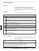
C–CCP Backplane
Troubleshooting Procedure
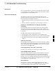
The following table provides a standard procedure for troubleshooting
problems that appear to be related to a defective C–CCP backplane. The
table is broken down into possible problems and steps which should be
taken in an attempt to find the root cause.
It is important to note that all steps be followed before
replacing ANY C–CCP backplane.
IMPORTANT
*
6