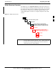
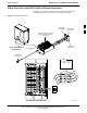
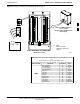
Preparing the LMF 68P09255A69-3 Folder Structure Overview The LMF uses a :\ folder that contains all of the essential data for installing and maintaining the BTS. The following list outlines the folder structure for LMF. Except for the bts-nnn folders, these folders are created as part of the LMF installation. Refer to the CDMA LMF Operator’s Guide for a complete description of the folder structure. Figure 3-1: LMF Folder Structure (C:) 3 x:\ folder cdma folder
Span Lines - Interface and Isolation 68P09255A69-3 Span Lines - Interface and Isolation T1/E1 Span Interface NOTE At active sites, the OMC-R/CBSC must disable the BTS and place it out of service (OOS). DO NOT remove the span line cable connectors until the OMC-R/CBSC has disabled the BTS. Each frame is equipped with one 50-pair punchblock for spans, customer alarms, remote GPS, and BTS frame alarms. See Figure 3-4 and refer to Table 3-6 for the physical location and punchdown location information.
Span Lines - Interface and Isolation 68P09255A69-3 T1/E1 Span Isolation Table 3-5 describes the action required for span isolation. Table 3-5: T1/E1 Span Isolation Step Action 1 Have the OMCR/CBSC place the BTS OOS. 2 To disable the span lines, locate the connector for the span or spans which must be disabled and remove the respective connector from the applicable SCCP cage Span I/O board (Figure 3-2).
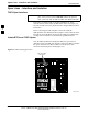
Span Lines - Interface and Isolation 68P09255A69-3 A PC using the AT 9-pin interface A modem using the 9-pin connector Other shelves in a daisy chain Figure 3-3: Rear and Front View of CSU Shelf To/From Network To/From GLI To/From Network To/From GLI 3 Rear View SLOT 1 SLOT 2 DCE Connector (Craft Port) CSU Modules Front View 3-14 1X SC 4812ET Lite BTS Optimization/ATP Software Release 2.16.1.
Span Lines - Interface and Isolation 68P09255A69-3 Alarm, Span Line, and RGPS Cable Pin/Signal Information See Figure 3-4 and refer to Table 3-6 for the physical location and punchdown location information for the 50-pair punchblock.
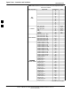
Span Lines - Interface and Isolation 68P09255A69-3 Table 3-6: Punchdown Location for Stand-alone and Companion Frame 50-Pair Punch Block Site Component Signal Name NOT USED 3 LFR/HSO PILOT BEACON CUSTOMER OUTPUTS / INPUTS LFR_HSO_GND EXT_IPPS_POS EXT_IPPS_NEG CAL_+ CAL_LORAN_ + LORAN_ Pilot Beacon Alarm - Minor Pilot Beacon Alarm - Rtn Pilot Beacon Alarm - Major Pilot Beacon Control - NO Pilot Beacon Control-COM Pilot Beacon Control - NC Customer Outputs 1 - NO Customer Outputs 1 - COM Customer Out
Span Lines - Interface and Isolation 68P09255A69-3 Table 3-6: Punchdown Location for Stand-alone and Companion Frame 50-Pair Punch Block Site Component SPAN Signal Name RCV_TIP_A RCV_RING_A XMIT_TIP_A XMIT_RING_A RCV_TIP_B RCV_RING_B XMIT_TIP_B XMIT_RING_B RCV_TIP_C RCV_RING_C XMIT_TIP_C XMIT_RING_C RCV_TIP_D RCV_RING_D XMIT_TIP_D XMIT_RING_D RCV_TIP_E RCV_RING_E XMIT_TIP_E XMIT_RING_E RCV_TIP_F RCV_RING_F XMIT_TIP_F XMIT_RING_F For Frames without RGD Expansion (20-pair) Punchblock See Table 3-7 RGPS F
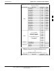
Span Lines - Interface and Isolation 68P09255A69-3 Table 3-7: 50-Pair Punch Block RGPS Punchdown Location for RGPS Non-Expansion Frames (Input from RGPS Receiver) and Secondary RGPS Expansion Frames (Input from RGPS Expansion Primary Frame 20-pair Punchblock) Site Component RGPS For frames without RGD Expansion (20-pair) Punchblock 3 Signal Name GPS_POWER_A+ GPS_POWER_AGPS_POWER_B+ GPS_POWER_BGPS_TX+ GPS_TXGPS_RX+ GPS_RXSignal Ground Master Frame GPS_1pps+ GPS_1pps- Punchdown 42T 42R 43T 43R 44T 44R
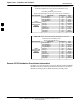
Span Lines - Interface and Isolation 68P09255A69-3 Figure 3-5: 20-pair Punchblock with RGD Module Punchdowns 1T 1R 2T 2R 3 Rear of RGPS Expansion Primary Frame (Power Entry Compartment Door Open) 1T 1R 2T 2R LEGEND 1T = PAIR 1 - TIP 1R = PAIR 1 -RING ” ” ” ” ” ” RGD (All interconnect cabling not shown for clarity.
LMF to BTS Connection 68P09255A69-3 LMF to BTS Connection Connect the LMF to the BTS The LMF computer may be connected to the LAN A or B connector located behind the frame lower air intake grill. Figure 3-6 below shows the general location of these connectors. LAN A is considered the primary LAN.
Using the LMF 68P09255A69-3 Using the LMF Basic LMF Operation LMF Coverage in This Publication - The LMF application program supports maintenance of both CDMA and SAS BTSs. All references to the LMF in this publication are to the CDMA portion of the program.
Using the LMF 68P09255A69-3 RFDS Display - If an RFDS is included in the CDF file, an RFDS tab labeled with “RFDS,” a dash and the BTS number-frame number combination (for example, RFDS-812-1 ) will be displayed. Logging Into a BTS Logging into a BTS establishes a communication link between the BTS and the LMF. An LMF session can be logged into only one BTS at a time.
Using the LMF 68P09255A69-3 Table 3-11: BTS GUI Login Procedure Step Action 3 Double click on CDMA (in the Available Base Stations pick list). 4 Click on the desired BTS number. 5 Click on the Network Login tab (if not already in the forefront). 6 Enter correct IP address (normally 128.0.0.2) for a field BTS, if not correctly displayed in the IP Address box. 7 Type in the correct IP Port number (normally 9216) if not correctly displayed in the IP Port box. 8 Click on Ping.
Using the LMF 68P09255A69-3 BTS Login from the CLI Environment Follow the procedures in Table 3-12 to log into a BTS when using the CLI environment. NOTE If the CLI and GUI environments are to be used at the same time, the GUI must be started first and BTS login must be performed from the GUI. Refer to Table 3-11 to start the GUI environment and log into a BTS.
Using the LMF 68P09255A69-3 Logging Out Logging out of a BTS is accomplished differently for the GUI and CLI operating environments. NOTE The GUI and CLI environments use the same connection to a BTS. If a BTS is logged into in both the GUI and CLI environments at the same time, logging out of the BTS in either environment will log out of it for both. When either a login or logout is performed in the CLI window, there is no GUI indication that the login or logout has occurred.
Using the LMF 68P09255A69-3 Logging Out of a BTS from the CLI Environment Follow the procedure in Table 3-14 to logout of a BTS when using the CLI environment. Table 3-14: BTS CLI Logout Procedure Step Action NOTE If the BTS is also logged into from a GUI running at the same time and further work must be done with it in the GUI, proceed to step 2. 1 3 Log out of a BTS by entering the following command: logout bts- A response similar to the following will be displayed: LMF> 13:24:51.
Using the LMF 68P09255A69-3 Table 3-15: Establishing MMI Communication Step Action 2b - In the LMF Options dialog box, click the Disconnect Port button on the Serial Connection tab. 3 Start the named HyperTerminal connection for MMI sessions by double clicking on its Windows desktop shortcut.
Pinging the Processors 68P09255A69-3 Pinging the Processors Pinging the BTS For proper operation, the integrity of the Ethernet LAN A and B links must be verified. Figure 3-8 represents a typical BTS Ethernet configuration for an SC4812ET Lite stand-alone or companion frame. The drawing depicts cabling and termination for both the A and B LANs.
Pinging the Processors 68P09255A69-3 NOTE The Ethernet LAN A and B cables and/or terminations must be installed on each frame/enclosure external LAN connector before performing this test. All other processor board LAN connections are made through the backplanes. Table 3-16: Pinging the Processors Step Action 1 If this is a first-time communication with a newly-installed frame or a GLI card which has been replaced, perform the procedure in Table 6-3 and then return to step 2.
Pinging the Processors 68P09255A69-3 Table 3-16: Pinging the Processors Step 14 Action If ping was unsuccessful after restarting the LMF computer, press the MGLI front panel reset pushbutton and perform steps 7 through 10 again. NOTE Refer to Table 6-1 if ping was unsuccessful after resetting the MGLI. 15 After the BTS has been successfully pinged, be sure the 50Ω termination was replaced on the BTS frame LAN B IN connector in the power entry compartment (Figure 3-8).
Download the BTS 68P09255A69-3 Download the BTS Overview Before a BTS can operate, each equipped device must contain device initialization (ROM) code. ROM code is loaded in all devices during manufacture, factory repair, or, for software upgrades, from the CBSC using the DownLoad Manager (DLM). Device application (RAM) code and data must be downloaded to each equipped device by the user before the BTS can be made fully functional for the site where it is installed.
Download the BTS 68P09255A69-3 When code is downloaded to an MGLI or GLI, the LMF automatically also downloads data and then enables the MGLI. When enabled, the MGLI will change to INS_ACT (bright green). A redundant GLI will not be automatically enabled and will remain OOS_RAM (yellow). When the redundant GLI is manually commanded to enable through the LMF, it will change state to INS_SBY (olive green). For non-GLI devices, data must be downloaded after RAM code is downloaded.
Download the BTS 68P09255A69-3 Table 3-17: Verify GLI ROM Code Loads Step Action 4a - Log out of the BTS as described in Table 3-13 or Table 3-14, as applicable. 4b - Disconnect the LMF computer. 4c - Reconnect the span lines as described in Table 5-7. 4d - Have the CBSC download the correct ROM code version to the BTS devices.
Download the BTS 68P09255A69-3 Download RAM Code and Data to Non-GLI Devices Downloads to non-GLI devices can be performed individually for each device or all installed devices can be downloaded with one action. NOTE 3 - CSM devices are RAM code-loaded at the factory. RAM code is downloaded to CSMs only if a newer software version needs to be loaded. - When downloading to multiple devices, the download may fail for some of the devices (a time-out occurs).
Download the BTS 68P09255A69-3 LFR (only for source 2 & 3) 10 MHz (only for source 2 & 3) NONE (only for source 2 & 3) Prerequisites MGLI is INS_ACT (bright green) CSM is OOS_RAM (yellow) or INS_ACT (bright green) Table 3-20: Select CSM Clock Source Step Action 1 Display the CSM cage view in the LMF by clicking on the CSM area of the SCCP shelf in the picture of the BTS frame.
Download the BTS 68P09255A69-3 Table 3-21: Enable CSMs Step 3 Action Click OK to close the status report window. NOTE The board in slot CSM 1 interfaces with the GPS receiver (either on-board or remote). The enable sequence for this board can take up to one hour (see below). FAIL may be shown in the status report table for a slot CSM 1 enable action. If Waiting For Phase Lock is shown in the Description field, do not cancel the enable process.
Download the BTS 68P09255A69-3 Enable MCCs This procedure configures the MCC and sets the “tx fine adjust” parameter. The “tx fine adjust” parameter is not a transmit gain setting, but a timing adjustment that compensates for the processing delay in the BTS (approximately 3 mS). Follow the steps outlined in Table 3-22 to enable the MCCs installed in the SCCP shelves. NOTE The MGLI and CSM must be downloaded and enabled, prior to downloading and enabling an MCC.
CSM System Time - GPS & LFR/HSO Verification 68P09255A69-3 CSM System Time - GPS & LFR/HSO Verification Clock Synchronization Manager (CSM) Sub-system Description Overview - Each BTS CSM sub-system features two CSM boards per RFMF. The primary function of the CSM cards is to maintain CDMA system time. GPS is used as the primary timing reference and synchronizes the entire cellular system. In typical operation, the primary CSM locks its Digital Phase Locked Loop (DPLL) circuits to GPS signals.
CSM System Time - GPS & LFR/HSO Verification 68P09255A69-3 Timing Source Fault Management - Fault management has the capability of switching between the GPS synchronization source and the LFR/HSO backup source in the event of a GPS receiver failure. During normal operation, the card in slot CSM 1 selects GPS as the primary timing source (Table 3-24). The source selection can also be overridden via the LMF or by the system software.
CSM System Time - GPS & LFR/HSO Verification 68P09255A69-3 CSM Frequency Verification The objective of this procedure is the initial verification of the Clock Synchronization Module (CSM) cards before performing the RF path verification tests. Test Equipment Setup (GPS & LFR/HSO Verification) Follow the steps outlined in Table 3-23 to set up test equipment.
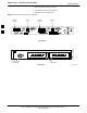
CSM System Time - GPS & LFR/HSO Verification 68P09255A69-3 Figure 3-9: CSM MMI Terminal Connection REFERENCE OSCILLATOR CSM card shown removed from frame MMI SERIAL PORT 3 EVEN SECOND TICK TEST POINT REFERENCE GPS RECEIVER ANTENNA INPUT ANTENNA COAX CABLE GPS RECEIVER 19.6 MHZ TEST POINT REFERENCE (NOTE 1) NULL MODEM BOARD (TRN9666A) 9-PIN TO 9-PIN RS-232 CABLE FW00372 LMF NOTEBOOK DB9-TO-DB25 ADAPTER RS-232 SERIAL MODEM CABLE COM1 NOTES: 1.
CSM System Time - GPS & LFR/HSO Verification 68P09255A69-3 Table 3-24: GPS Initialization/Verification Step Action 1 To verify that Clock alarms (0000), Dpll is locked and has a reference source, and GPS self test passed messages are displayed within the report, issue the following MMI command bstatus - The system will display a response similar to the following: Clock Alarms (0000): DPLL is locked and has a reference source.
68P09255A69-3 CSM System Time - GPS & LFR/HSO Verification Table 3-24: GPS Initialization/Verification Step Action 3 HSO information (underlined text above, verified from left to right) is usually the #1 reference source. If this is not the case, have the OMCR determine the correct BTS timing source has been identified in the database by entering the display bts csmgen command and correct as required using the edit csm csmgen refsrc command.
CSM System Time - GPS & LFR/HSO Verification 68P09255A69-3 Table 3-24: GPS Initialization/Verification Step 5 Action Enter the following command at the CSM> prompt to verify that the GPS receiver is in tracking mode.
CSM System Time - GPS & LFR/HSO Verification 68P09255A69-3 Table 3-24: GPS Initialization/Verification Step 7 Action If steps 1 through 6 pass, the GPS is good. NOTE If any of the above mentioned areas fail, verify that: - If Initial position accuracy is “estimated” (typical), at least 4 satellites must be tracked and visible (1 satellite must be tracked and visible if actual lat, log, and height data for this site has been entered into CDF file).
CSM System Time - GPS & LFR/HSO Verification 68P09255A69-3 LORAN-C Initialization/Verification Table 3-25: LORAN-C Initialization/Verification Step 1 Action At the CSM> prompt, enter lstatus to verify that the LFR is in tracking mode.
CSM System Time - GPS & LFR/HSO Verification 68P09255A69-3 Table 3-25: LORAN-C Initialization/Verification Step Action Note 2 Verify the following LFR information (highlighted above in boldface type): - Locate the “dot” that indicates the current phase locked station assignment (assigned by MM). - Verify that the station call letters are as specified in site documentation as well as M X Y Z assignment. - Verify the S/N ratio of the phase locked station is greater than 8.
Test Equipment Set-up 68P09255A69-3 Test Equipment Set-up Connecting Test Equipment to the BTS The following types of test equipment are required to perform calibration and ATP tests: LMF Communications system analyzer model supported by the LMF Power meter model supported by the LMF (required when using the HP 8921A/600 and Advantest R3465 analyzers) Non-radiating transmit line termination load Directional coupler and in-line attenuator RF cables and adapters 3 Refer to Table 3-26 for an
Test Equipment Set-up 68P09255A69-3 Supported Test Equipment CAUTION To prevent damage to the test equipment, all transmit (TX) test connections must be through a 30 dB directional coupler plus a 20 dB in-line attenuator for both the 800 MHz and 1.9 GHz BTSs.
Test Equipment Set-up 68P09255A69-3 Test Equipment Connection Charts To use the following charts to identify necessary test equipment connections, locate the communications system analyzer being used in the COMMUNICATIONS SYSTEM ANALYZER columns, and read down the column. Where a dot appears in the column, connect one end of the test cable to that connector. Follow the horizontal line to locate the end connection(s), reading up the column to identify the appropriate equipment and/or BTS connector.
Test Equipment Set-up 68P09255A69-3 CDMA2000 1X/IS-95A/B-capable Test Equipment Connections Table 3-27 depicts the interconnection requirements for currently available test equipment supporting both CDMA 2000 1X and IS-95A/B which meets Motorola standards and is supported by the LMF. Table 3-27: CDMA2000 1X/IS-95A/B Test Equipment Interconnection COMMUNICATIONS SYSTEM ANALYZER SIGNAL EVEN SECOND SYNCHRONIZATION 19.
Test Equipment Set-up 68P09255A69-3 Equipment Warm-up NOTE Warm-up BTS equipment for a minimum of 60 minutes prior to performing the BTS optimization procedure. This assures BTS stability and contributes to optimization accuracy. - Time spent running initial or normal power-up, hardware/firmware audit, and BTS download counts as warm-up time. WARNING Before installing any test equipment directly to any BTS TX OUT connector, verify there are no CDMA channels keyed.
Test Equipment Set-up 68P09255A69-3 Figure 3-10: IS- 95A/B Cable Calibration Test Setup - CyberTest, Agilent 8935, Advantest R3465, and HP 8921A SUPPORTED TEST SETS CALIBRATION SET UP A. SHORT CABLE CAL Motorola CyberTest ÏÏÏ ÏÏÏÌ ANT IN SHORT CABLE TEST SET 3 RF GEN OUT Note: The 30 dB directional coupler is not used with the Cybertest test set. The TX cable is connected directly to the Cybertest test set. B.
Test Equipment Set-up 68P09255A69-3 Figure 3-11: IS-95A/B and CDMA 2000 1X Cable Calibration Test Setup - Agilent E4406A/E4432B and Advantest R3267/R3562 CALIBRATION SET UP SUPPORTED TEST SETS A. SHORT CABLE CAL Agilent E4432B (Top) and E4406A (Bottom) SHORT CABLE TEST SET 3 RF OUTPUT 50 Ω B.
Test Equipment Set-up 68P09255A69-3 Figure 3-12: CDMA2000 1X Cable Calibration Test Setup - Agilent 8935/E4432B CALIBRATION SET UP SUPPORTED TEST SETS A. SHORT CABLE CAL Agilent E4432B (Top) and 8935 Series E6380A (Bottom) SHORT CABLE ÁÁ ÁÁ ÁÁ ÁÁ TEST SET RF OUTPUT 50 Ω 3 B. RX TEST SETUP FOR TRDC N-N FEMALE ADAPTER RX CABLE ANT IN SHORT CABLE NOTE: TEST SET 10 MHZ IN ON REAR OF SIGNAL GENERATOR IS CONNECTED TO 10 MHZ REF OUT ON SIDE OF CDMA BASE STATION TEST SET (FIGURE F-15). D.
Test Equipment Set-up 68P09255A69-3 Set-up for TX Calibration Figure 3-13 and Figure 3-14 show the test set connections for TX calibration. Figure 3-13: TX Calibration Test Setup - CyberTest (IS-95A/B) and Agilent 8935 (IS-95A/B and CDMA2000 1X) TEST SETS TRANSMIT (TX) SET UP Motorola CyberTest ÏÏÏ ÏÏÏ ÏÏÏÌ 3 FRONT PANEL POWER SENSOR NOTE: IF BTS IS EQUIPPED WITH DRDCS (DUPLEXED RX/TX SIGNALS), CONNECT THE TX TEST CABLE TO THE DRDC ANTENNA CONNECTOR. COMMUNICATIONS SYSTEM ANALYZER 100-W ATT (MIN.
Test Equipment Set-up 68P09255A69-3 Figure 3-14: TX Calibration Test Setup - Using Power Meter TEST SETS NOTE: THE HP8921A AND ADVANTEST R3465 CANNOT BE USED FOR TX CALIBRATION. A POWER METER MUST BE USED. TRANSMIT (TX) SET UP POWER SENSOR NOTE: IF BTS IS EQUIPPED WITH DRDCS (DUPLEXED RX/TX SIGNALS), CONNECT THE TX TEST CABLE TO THE DRDC ANTENNA CONNECTOR. POWER METER 100-W ATT (MIN.) NON-RADIA TING RF LOAD 3 TX TEST CABLE DIRECTIONAL COUPLER (30 DB) 50 Ω TERM .
Test Equipment Set-up 68P09255A69-3 Figure 3-15: TX Calibration Test Setup - Agilent E4406A and Advantest R3567 (IS-95A/B and CDMA2000 1X) TEST SETS TRANSMIT (TX) SET UP Agilent E4406A POWER SENSOR NOTE: IF BTS IS EQUIPPED WITH DRDCS (DUPLEXED RX/TX SIGNALS), CONNECT THE TX TEST CABLE TO THE DRDC ANTENNA CONNECTOR. COMMUNICATIONS SYSTEM ANALYZER RF INPUT 50 Ω OR INPUT 50 Ω 100-W ATT (MIN.
Test Equipment Set-up 68P09255A69-3 Set-up for ATP Figure 3-16 and Figure 3-17 show the test set connections for ATP tests. Figure 3-16: IS-95A/B ATP Test Set-up, TRDC Shown - CyberTest, Advantest R3465, and Agilent 8935 TEST SETS Optimization/ATP SET UP Motorola CyberTest SYNC MONITOR EVEN SEC TICK PULSE REFERENCE FROM CSM BOARD FREQ MONITOR 19.
Test Equipment Set-up 68P09255A69-3 Figure 3-17: IS-95A/B ATP Test Setup - HP 8921A TEST SETS Optimization/ATP SET UP Hewlett Packard Model HP 8921A W/PCS Interface (for 1900 MHz) SYNC MONITOR EVEN SEC TICK PULSE REFERENCE FROM CSM BOARD IMPORTANT: WHEN PERFORMING FER TEST ON COMPANION FRAME DIVERSITY RX, CONNECT RX TEST CABLE TO RX ANTENNA PORT ON COLLOCATED COMPANION FRAME. FREQ MONITOR 19.
Test Equipment Set-up 68P09255A69-3 Figure 3-18: IS-95A/B and CDMA2000 1X ATP Test Setup With DRDCs - Agilent Test Equipment TEST SETS Optimization/ATP SET UP Agilent E4432B (Top) and 8935 Series E6380A (Bottom) RF OUTPUT 50 Ω IMPORTANT: WHEN PERFORMING FER TEST ON COMPANION FRAME DIVERSITY RX, CONNECT RX TEST CABLE TO ANTENNA PORT ON COLLOCATED COMPANION FRAME. RF OUTPUT 50 Ω 10 MHZ IN PATTERN TRIG IN RX TEST CABLE Á ÁÁ Á SIGNAL GENERATOR RF IN/OUT OR RF INPUT 50 Ω 100-W ATT (MIN.
Test Equipment Set-up 68P09255A69-3 Figure 3-19: IS-95A/B and CDMA2000 1X ATP Test Setup With DRDCs - Advantest R3267/3562 Test Equipment TEST SETS Optimization/ATP SET UP IMPORTANT: WHEN PERFORMING FER TEST ON COMPANION FRAME DIVERSITY RX, CONNECT RX TEST CABLE TO ANTENNA PORT ON COLLOCATED COMPANION FRAME. Advantest R3267 (Top) and R3562 (Bottom) TO EXT TRIG ON REAR OF SPECTRUM ANALYZER SIGNAL GENERATOR MOD TIME BASE IN SYNTHE REF IN EXT TRIG IN GPIB RX TEST CABLE 100-W ATT (MIN.
Test Equipment Set-up 68P09255A69-3 Figure 3-20: IS-95A/B and CDMA2000 1X ATP Test Setup With TRDCs - Agilent Test Equipment TEST SETS Optimization/ATP SET UP IMPORTANT: WHEN PERFORMING FER TEST ON COMPANION FRAME DIVERSITY RX, CONNECT RX TEST CABLE TO RX ANTENNA PORT ON COLLOCATED COMPANION FRAME. Agilent E4432B (Top) and 8935 Series E6380A (Bottom) RX TEST CABLE SIGNAL GENERATOR RF OUTPUT 50 Ω 10 MHZ IN RF OUTPUT 50 Ω ÁÁ Á Á ÁÁ ÁÁ RF IN/OUT OR RF INPUT 50 Ω 100-W ATT (MIN.
Test Equipment Set-up 68P09255A69-3 Figure 3-21: IS-95A/B and CDMA2000 1X ATP Test Setup With TRDCs - Advantest R3267/3562 Test Equipment TEST SETS Optimization/ATP SET UP IMPORTANT: WHEN PERFORMING FER TEST ON COMPANION FRAME DIVERSITY RX, CONNECT RX TEST CABLE TO RX ANTENNA PORT ON COLLOCATED COMPANION FRAME.
Test Set Calibration 68P09255A69-3 Test Set Calibration Background Proper test equipment calibration helps to ensure accurate BTS optimization and acceptance testing by assuring that the test equipment and associated cables do not introduce measurement errors. NOTE If the test equipment set (see the Terms and Abbreviations section of Chapter 1) being used to optimize or test the BTS has been calibrated and maintained as a set, this procedure does not need to be performed.
Test Set Calibration 68P09255A69-3 Power Meters - Manual power meter calibration procedures to be performed prior to automated calibration are included in the Equipment Calibration section of Appendix F. Cable Calibration - Manual cable calibration procedures using the HP 8921A and Advantest R3465 communications system analyzers are provided in the Manual Cable Calibration section of Appendix F, if needed. GPIB Addresses GPIB addresses can range from 1 through 30.
Test Set Calibration 68P09255A69-3 Manually Selecting Test Equipment in a Serial Connection Tab Test equipment can be manually specified before or after the test equipment is connected. The LMF does not attempt to verify the test equipment is actually detected when manual selection is specified. Follow the procedure in Table 3-28 to manually select test equipment.
Test Set Calibration 68P09255A69-3 Automatically Selecting Test Equipment in the Serial Connection Tab When using the auto-detection feature to select test equipment, the LMF determines which test equipment items are actually communicating with LMF. Follow the procedure in Table 3-29 to use the auto-detection feature. Table 3-29: Selecting Test Equipment Using Auto-Detect Step 3 Action 1 In the LMF window menu bar, click Tools and select Options... from the pull-down menu.
Test Set Calibration 68P09255A69-3 Calibrating Test Equipment The LMF Calibrate Test Equipment function zeros the power measurement level of the test equipment item that is to be used for TX calibration and audit. If both a power meter and an analyzer are connected (for example, an HP 437 and an HP8921A/600), only the power meter is zeroed. NOTE The Agilent E4406A transmitter tester does not support power measurement level zeroing.
Test Set Calibration 68P09255A69-3 2. Measure the loss of the short cable plus the RX test cable configuration. The RX test cable configuration normally consists only of a coax cable with type-N connectors that is long enough to reach from the BTS RX connector to the test equipment. When the BTS antenna connectors carry duplexed TX and RX signals, a directional coupler and, if required by BTS type, an additional attenuator are also required for the RX test cable configuration.
Test Set Calibration 68P09255A69-3 Table 3-31: Test Cable Configuration Calibration with a Communications System Analyzer Step 2 Action Enter one or more channel numbers in the Channels box. NOTE Multiple channel numbers must be separated by a comma with no spaces (for example, 200,800). When two or more channel numbers are entered, the cables will be calibrated for each channel. Interpolation will be accomplished for other channels, as required, for TX calibration.
Test Set Calibration 68P09255A69-3 Figure 3-22: Calibration Setup for TX Test Cable Configuration and Duplexed RX Test Cable Configuration Using Signal Generator and Spectrum Analyzer THIS WILL CONNECT TO THE BTS TX ANTENNA CONNECTOR DURING TX CALIBRATION AND TO THE TX/RX ANTENNA CONNECTORS DURING ATP TESTS. Signal Generator Spectrum Analyzer 40W NON-RADIATING RF LOAD Signal Generator 3 A SHORT TEST CABLE 50 OHM TERMINATION Spectrum Analyzer 20DB 20 W IN-LINE ATTENUATOR FOR 1.
Test Set Calibration 68P09255A69-3 Table 3-33: Calibrating Non-Duplexed RX Test Cable Configuration Using a Signal Generator and Spectrum Analyzer Step Action Calibration factor = (value measured with detail “A” setup) - (value measured with detail “B” setup) Example: Cal factor = -12 dBm - (-14 dBm) = 2 dB 5 NOTE The short test cable is used for test equipment setup calibration only. It is not part of the final test setup. After calibration is completed, do not re-arrange any cables.
Test Set Calibration 68P09255A69-3 Setting Cable Loss Values Cable loss values for TX and RX test cable configurations are normally set by accomplishing automatic cable calibration using the LMF and the applicable test equipment. The LMF stores the measured loss values in the cable loss files. The cable loss values can also be set or changed manually. CAUTION If cable calibration was performed without using the LMF, cable loss values must be manually entered in the LMF database.
Test Set Calibration 68P09255A69-3 Setting TX Coupler Loss Value If an in-service TX coupler is installed, the coupler loss must be manually entered so it will be included in the LMF TX calibration and audit calculations. Prerequisites LMF is logged into the BTS Path loss, in dB, of the TX coupler must be known Table 3-35: Setting TX Coupler Loss Values Step 3 Action 1 Click Util in the BTS menu bar, and select Edit > Coupler Loss... in the pull-down menus.
Bay Level Offset Calibration 68P09255A69-3 Bay Level Offset Calibration Purpose of Bay Level Offset Calibration Bay Level Offset (BLO) calibration is the central activity of the optimization process. BLO calibration compensates for normal equipment variations within the BTS RF paths and assures the correct transmit power is available at the BTS antenna connectors to meet site performance requirements.
Bay Level Offset Calibration 68P09255A69-3 frame through the RX expansion out connectors (RX EXPANSION 1A, 2A, or 3A in Figure 1-9 or Figure 1-10). The signal travels through the inter-frame diversity RX cables, into the RX expansion in ports (RX EXPANSION 1B, 2B, or 3B in Figure 1-9 or Figure 1-10) of the companion frame, through the Expansion MPC (EMPC) in SCCP cage slot MPC-2, the CIO, and terminates at a backplane BBX slot in the SCCP shelf.
Bay Level Offset Calibration NOTE 68P09255A69-3 Due to the size of the file, Motorola recommends printing out a copy of a bts- #.cal file and referring to it for the following descriptions. CAL File Organization The CAL file is subdivided into three sections called “slot Blocks”. These are: 1. Slot[1] Block which contains the calibration data for the six primary BBX slots. 2. Slot[20] Block which contains the calibration data for the redundant BBX (see Table 3-37). 3.
Bay Level Offset Calibration 68P09255A69-3 The second view of the array is shown in Table 3-37. This view shows the assignment of calibration entries in each branch to each BBX slot, carrier, and sectorization. Three sectors are allowed for an SC4812ET Lite frame. Table 3-37: SC4812ET Lite bts- #.
Bay Level Offset Calibration 68P09255A69-3 from 2500 to 27500 (2500 corresponds to -125 dBm and 27500 corresponds to +125 dBm). - The ten calibration points for each slot-branch combination must be stored in order of increasing frequency. If less than ten points (frequencies) are calibrated, the BLO data for the highest frequency calibrated is written into the remainder of the ten points for that slot-branch.
Bay Level Offset Calibration 68P09255A69-3 Table 3-38: Set Up Test Equipment for RF Path Calibration Step 4 Action ! CAUTION To prevent damage to the test equipment, all transmit (TX) test connections must be via the 30 dB directional coupler for 800 MHz or via a 30 dB coupler with a 20 dB in-line attenuator for 1900 MHz. For TX path calibration, connect the test equipment as shown in Figure 3-13, Figure 3-14, or Figure 3-15, depending on the communications analyzer being used.
Bay Level Offset Calibration 68P09255A69-3 TX Calibration and the LMF The LMF Tests > TX > TX Calibration... and Tests > All Cal/Audit... selections perform TX BLO calibration testing for installed BBX(s). The All Cal/Audit... selection initiates a series of actions to perform TX calibration, and if calibration is successful, download BLO and perform TX audit. The TX Calibration... selection performs only TX calibration. When TX Calibration...
Bay Level Offset Calibration 68P09255A69-3 Test Pattern Drop-down Pick List Test Pattern Default and Descriptions - Pilot is shown as the default setting in this picklist box. The full range of available selections and their descriptions are as follows: Standard - performs calibration or audit using pilot, paging, synch, and six traffic channels with IS-97-specified gain. This pattern setting should be used for all non-in-service calibrations and audits.
Bay Level Offset Calibration 68P09255A69-3 TX Calibration 3 WARNING Before installing any test equipment directly to any BTS TX OUT connector, first verify no CDMA channels are keyed. Failure to do so can result in serious personal injury and/or equipment damage. CAUTION Always wear an approved anti-static wrist strap while handling any circuit card or module. If this is not done, there is a high probability that the card or module could be damaged by ESD.
Bay Level Offset Calibration 68P09255A69-3 Table 3-40: All Cal/Audit Procedure Step Action 1 If it has not already been done, configure test equipment for TX calibration by following the procedure in Table 3-38. 2 Click on the BBX(s) to be calibrated. 3 If the Test Pattern to be used is Standard, CDFPilot, or CDF, select at least one MCC (refer to “Test Pattern Drop-down Pick List” under “TX Calibration and the LMF” in this section).
Bay Level Offset Calibration 68P09255A69-3 TX Calibration Procedure The LMF TX calibration procedure performs only the BLO calibration on the TX paths. The BLO download and TX audit functions must be performed separately when this method is chosen to perform calibration. Prerequisites Before running this test, be sure that the following have been done: The card in slot CSM 1, GLIs, MCCs, and BBXs have correct code and data loads. 3 Primary CSM and MGLI are INS_ACT (bright green).
Bay Level Offset Calibration 68P09255A69-3 Table 3-41: TX Calibration Procedure Step Action 7 If at least one MCC was selected in Step 3, select the appropriate transfer rate (1 = 9600, 3 = 9600 1X) from the drop-down list in the Rate Set box. NOTE The rate selection of 3 is only available if 1X cards are selected for the test. 8 If Verify BLO is to be used during the calibration, leave the checkbox checked (default).
Bay Level Offset Calibration 68P09255A69-3 Table 3-42: Download BLO Step Action 1 Select the BBX(s) to be downloaded. 2 Click Device in the BTS menu bar, and select Download > BLO from the pull-down menus. - A status report window displays the result of the download. NOTE 3 Selected device(s) do not change color when BLO is downloaded. Click OK to close the status report window.
Bay Level Offset Calibration 68P09255A69-3 Prerequisites Before running this test, the following should be done: The card in slot CSM 1, GLIs, BBXs have correct code load. Primary CSM and MGLI are INS_ACT (bright green). All BBXs are OOS_RAM (yellow). Test equipment and test cables are calibrated and connected for TX BLO calibration. LMF is logged into the BTS.
Bay Level Offset Calibration 68P09255A69-3 Exception Handling In the event of a failure, the calibration procedure displays a FAIL message in the status report window and provides information in the Description field. Re-check the test setup and connections and re-run the test. If the tests fail again, note specifics about the failure, and refer to Chapter 6, Troubleshooting. Create CAL File The LMF Create Cal File function gets the BLO data from BBXs and creates/updates the CAL file for the BTS.
RFDS Set-up and Calibration 68P09255A69-3 RFDS Set-up and Calibration RFDS Description The optional RFDS is used to perform RF tests of the site from the CBSC or from the LMF.
RFDS Set-up and Calibration 68P09255A69-3 Checking and Setting RFDS Parameters Follow the procedure in Table 3-45 to review and/or edit RFDS parameters. Table 3-45: RFDS Parameter Settings Step Action NOTE Log out of the BTS prior to perform this procedure. 1 3 Using a text editor, verify the following fields are set correctly in the bts-#.
RFDS Set-up and Calibration 68P09255A69-3 Table 3-45: RFDS Parameter Settings Step Action 5g - Click OK to close the status report window. 5h - Click on the MGLI. 5i - Click on Device in the BTS menu bar, and select Enable from the pull-down menu. -- A status report window shows the status of the operation. 5j - When the operation is complete, click OK to close the status report window. ! CAUTION When the MGLI changes to INS_ACT, data will automatically be downloaded to the RFDS.
RFDS Set-up and Calibration 68P09255A69-3 Table 3-45: RFDS Parameter Settings Step Action - Click OK to close the status report window. 8c NOTE If the LMF displays an error message, check the following: 3 Ensure AMR cable is correctly connected from the BTS to the RFDS. Verify RFDS has power. Verify RFDS status LED is green. Verify entries in RFDS fields of the bts-#.cdf file are correct (refer to step 1).
RFDS Set-up and Calibration 68P09255A69-3 Explanation of Parameters Used When Programming the TSU NAM Table 3-46 defines the parameters used when editing the tsu.nam file. Table 3-46: Definition of Parameters Access Overload Code Slot Index System ID Network ID These parameters are obtained from the switch. Primary Channel A Primary Channel B Secondary Channel A Secondary Channel B These parameters are the channels which are to be used in operation of the system.
RFDS Set-up and Calibration 68P09255A69-3 Valid NAM Ranges Table 3-47 provides the valid NAM field ranges. If any of the fields are missing or out-of-range, the RFDS will error out.
RFDS Set-up and Calibration 68P09255A69-3 Set Antenna Map Data The antenna map data must be entered manually if an RFDS is installed. Antenna map data does not need to be entered if an RFDS is not installed. The antenna map data is only used for RFDS tests and is required if an RFDS is installed. Prerequisite LMF is logged into the BTS Follow the procedure in Table 3-48 to set antenna map data for the RFDS.
RFDS Set-up and Calibration 68P09255A69-3 Set RFDS Configuration Data If an RFDS is installed, the RFDS configuration data must be manually entered. Prerequisite LMF is logged into the BTS NOTE The entered antenna# index numbers must correspond to the antenna# index numbers used in the antenna maps. Follow the procedure in Table 3-49 to set RFDS configuration data. 3 Table 3-49: Set RFDS Configuration Data Step Action 1 Click on Util in the BTS menu bar, and select Edit > RFDS Configuration...
RFDS Set-up and Calibration 68P09255A69-3 RFDS Calibration The RFDS Calibration option is used to calibrate the RFDS TX and RX paths. TX Path Calibration - For a TX antenna path calibration the BTS XCVR is keyed at a pre-determined power level and the BTS power output level is measured by the RFDS. The power level is then measured at the TX antenna directional coupler by the power measuring test equipment item being used (power meter or analyzer).
RFDS Set-up and Calibration 68P09255A69-3 RFDS Calibration Procedure Prerequisites Test equipment has been selected. Test equipment and test cables have been calibrated. TX calibration has been performed and BLO data has been downloaded to the BBXs. Test equipment and test cables are connected for TX calibration. Antenna map data has been entered for the site. BBXs are OOS-RAM. 3 Follow the procedure in Table 3-51 to perform RFDS calibration.
RFDS Set-up and Calibration 68P09255A69-3 Program TSU NAM The NAM must be programmed before it can receive and process test calls, or be used for any type of RFDS test. Prerequisites MGLI is INS_ACT (bright green). SUA is powered up and has a code load. Follow the procedure in Table 3-52 to program the TSU NAM. Table 3-52: Program NAM Procedure Step Action 1 In the LMF, select the RFDS tab. 2 Select the SUA by clicking on it.
Alarms Testing 68P09255A69-3 Alarms Testing Alarm Verification Alarms testing should be performed at a convenient point in the optimization/ATP process, since the LMF is necessary to ensure that the SC4812ET Lite is generating the appropriate alarms. The SC 4812ET Lite is capable of concurrently monitoring 10 customer defined input signals and four customer defined outputs, which interface to the 50-pair punchblock. All alarms are defaulted to “Not Equipped” during ATP testing.
Alarms Testing 68P09255A69-3 Alarm Testing Set-up Prepare for any alarm testing by following the procedures in Table 3-53. Table 3-53: Alarm Testing Preparation Step Action 1 If it has not already been done, refer to the procedure in Table 3-10 to connect the LMF computer terminal to the frame LAN A connector. 2 If it has not already been done, refer to Table 3-11 to start a GUI LMF session. 3 Click on Util in the BTS menu bar, and select Alarm Monitor... from the pull-down menu.
Alarms Testing 68P09255A69-3 AC Fail Alarm Table 3-56 gives instructions on testing the AC Fail Alarm. Table 3-56: AC Fail Alarm Step 1 Action NOTE - Back-up batteries must be installed when performing this test. - To prevent inadvertently shutting down the RF compartment electronics, the batteries should be charged before performing this test. 3 Set the ACLC MAIN circuit breaker to OFF.
Alarms Testing 68P09255A69-3 Single Rectifier Failure (Three Rectifier System) Table 3-58 gives instructions on testing single rectifier failure or minor alarm in a three (3) rectifier system (single-carrier system). Procedures in this test are for a frame configured for single carrier operation with rectifiers installed in rectifier shelf positions 1, 2, and 3, from left to right when facing the frame.
Alarms Testing 68P09255A69-3 Single Rectifier Failure (Four Rectifier System) Table 3-60 gives instructions on testing single rectifier failure or minor alarm in a four (4) rectifier system (two-carrier system). Table 3-60: Single Rectifier Fail or Minor Alarm, Two-Carrier System Step 1 Action ! CAUTION Only perform this test if the rectifier current load displayed on the AMP indicator on the MAP is 125 amps or less.
Alarms Testing 68P09255A69-3 Multiple Rectifier Failure (Four Rectifier System) Table 3-61 gives instructions on testing multiple rectifier failure or major alarm in a four (4) rectifier system (two-carrier system). Table 3-61: Multiple Rectifier Failure or Major Alarm, Two-Carrier System Step 1 Action ! CAUTION Only perform this test if the rectifier current load displayed on the AMP indicator on the MAP is 125 amps or less.
Alarms Testing 68P09255A69-3 Battery Over Temperature Alarm (Optional) CAUTION Use special care to avoid damaging insulation on cables, or damaging battery cases when using a heat gun. Table 3-62 gives instructions on testing the battery over-temperature alarm system. Table 3-62: Battery Over-Temperature Alarm Step 3 1 Action Use a low-powered heat gun to gently heat the battery over-temperature sensor (see location in Figure 3-24).
Alarms Testing 68P09255A69-3 Figure 3-24: Battery Over-Temperature Sensor 3 Bus Bar 6 AWG Cables Battery Overtemp Sensor Negative Temperature Compensation Sensor SC4812ETL0014-1 Aug 2002 1X SC 4812ET Lite BTS Optimization/ATP Software Release 2.16.1.
Alarms Testing 68P09255A69-3 Rectifier Over Temperature Alarm Table 3-63 gives instructions on testing the rectifier over-temperature alarm system. CAUTION Do not attempt to remove the MAP from the front of the frame to perform the following procedure, even if the frame is equipped with a MAP cable tray. MAP removal from the front requires complete site shut-down to avoid accidently shorting 27 Vdc to ground during the removal process.