Chapter 4 4 Automated Acceptance Test Procedures Aug 2002 1X SC 4812ET Lite BTS Optimization/ATP Software Release 2.16.1.
Automated Acceptance Test Procedure - Introduction 68P09255A69-3 Automated Acceptance Test Procedure - Introduction Introduction General The Acceptance Test Procedures (ATP) allow Cellular Field Engineers (CFEs) to run automated acceptance tests on all BTS subsystem devices equipped in the CDF using the LMF and the test equipment it supports. Test Reports The CFE can choose to save the results of ATP tests to a report file from which ATP reports are generated for later printing.
Automated Acceptance Test Procedure - Introduction 68P09255A69-3 In the unlikely event that the BTS passes these tests but has a forward link problem during normal operation, the CFE should then perform the additional TX tests for troubleshooting: TX spectral mask, TX rho, and TX code domain. ATP Test Options ATP tests can be run individually or as one of the following groups: All TX: TX tests verify the performance of the BTS transmit elements.
Automated Acceptance Test Procedure - Introduction WARNING 68P09255A69-3 1. All transmit connectors must be properly terminated for all ATP tests. 2. Before the FER is run, be sure that one of the following is done: - All transmitter connectors are properly terminated OR - All LPAs are turned OFF (circuit breakers pulled) Failure to observe these warnings may result in bodily injury or equipment damage.
Automated Acceptance Test Procedure - Introduction 68P09255A69-3 Disconnected companion frames: When inter-frame diversity RX cables are disconnected, connect test equipment for diversity RX ATP at the RX EXPANSION connectors 1B, 2B, or 3B on the frame under test. Refer to Figure 4-1 and Table 4-2. Be sure EMPC is selected before logging the LMF into the frame or FER will fail.
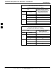
Automated Acceptance Test Procedure - Introduction 68P09255A69-3 Table 4-1: To Perform Companion Frame Diversity RX FER, Inter-frame RX Cables Connected (Set Multi-Channel Preselector to MPC) Sector Connect RX Test Cable to Collocated Companion Frame RX or Duplexed TX/RX ANTENNAS Connector 1 1A 2 2A 3 3A 1 1A 2 2A 3 3A On Carrier 1 2 4 Table 4-2: To Perform Companion Frame Diversity RX FER, Inter-frame RX Cables Disconnected (Set Multi-Channel Preselector to EMPC) Sector Connect RX Tes
Acceptance Tests - Test Set-up 68P09255A69-3 Acceptance Tests - Test Set-up Required Test Equipment The following test equipment is required: WARNING NOTE LMF Power meter (used with HP8921A/600 and Advantest R3465) Communications system analyzer Signal generator for FER testing (required for all communications system analyzers for 1X FER) - Before installing any test equipment directly to any BTS TX OUT connector, verify that there are no CDMA channels keyed.
Acceptance Tests - Test Set-up 68P09255A69-3 Companion frame All TX/RX, All RX, and FER for Diversity RX When performing All TX/RX, All RX, or FER ATP for companion frame diversity RX, perform the additional test equipment set-up procedures in Table 4-4. Table 4-4: Additional Diversity RX Test Set-up for Companion Frames Step Action 1 If the LMF is logged into the BTS, log out of the BTS.
Abbreviated (All-inclusive) Acceptance Tests 68P09255A69-3 Abbreviated (All-inclusive) Acceptance Tests All-inclusive Tests General - The all-inclusive acceptance tests are performed from the LMF GUI environment. These all-inclusive tests are called abbreviated ATPs because they execute various combinations of individual acceptance tests with a single command. This allows verification of multiple aspects of BTS performance while minimizing time needed for individual test set up and initiation.
Abbreviated (All-inclusive) Acceptance Tests 68P09255A69-3 All TX/RX ATP Test Follow the procedures in Table 4-5 to perform the abbreviated, all-inclusive transmit and receive test. Table 4-5: All TX/RX ATP Test Procedure Step Action 1 Set up the test equipment initially for abbreviated tests as described in Table 4-3.
Abbreviated (All-inclusive) Acceptance Tests 68P09255A69-3 Table 4-5: All TX/RX ATP Test Procedure Step Action 10 In the Test Pattern box, select the test pattern to use for the acceptance tests from the drop-down list (refer to “Test Pattern Drop-down Pick List” under “TX Calibration and the LMF” in the Bay Level Offset Calibration section of Chapter 3). 11 Click OK to display a status bar followed by a Directions pop-up window.
Abbreviated (All-inclusive) Acceptance Tests 68P09255A69-3 Table 4-6: All TX ATP Test Procedure Step Action 8 Click OK to display a status bar followed by a Directions pop-up window. 9 Follow cable connection directions as they are displayed, and click the Continue button to begin testing. - As the ATP process is completed, results will be displayed in the status report window. 10 Click the Save Results or Dismiss button.
Abbreviated (All-inclusive) Acceptance Tests 68P09255A69-3 Table 4-7: All RX ATP Test Procedure Step 8 Action In the Rate Set box, select the appropriate data rate (1=9600, 2=14400, 3=9600 1X) from the drop-down list. NOTE The Rate Set selection of 1 is only available if non-1X cards are selected for the test. The Rate Set selection of 3 is only available if 1X cards are selected for the test. 9 Enter the channel elements to be tested for the RX ATP in the Channel Element(s) box.
Individual Acceptance Tests 68P09255A69-3 Individual Acceptance Tests The following individual ATP tests can be used to evaluate specific aspects of BTS operation against individual performance requirements. All testing is performed using the LMF GUI environment. TX Testing TX tests verify any given transmit antenna path and output power control. All tests are performed using the external, calibrated test equipment. All measurements are made at the appropriate BTS TX OUT connector(s).
Individual Acceptance Tests 68P09255A69-3 BTS FER This test verifies the BTS receive FER on all traffic channel elements currently configured on all equipped MCCs (full rate at one percent FER) at an RF input level of -119 dBm on the main RX antenna paths using operator-selected, CDF-equipped MCCs and BBXs at the site. Diversity RX antenna paths are also tested using the lowest equipped MCC channel element ONLY.
TX Spectral Purity Transmit Mask Acceptance Test 68P09255A69-3 TX Spectral Purity Transmit Mask Acceptance Test Background Overview - This test verifies the spectral purity of each operator-selected BBX carrier keyed up at a specific frequency specified in the current CDF. All tests are performed using the external, calibrated test equipment controlled by the same command. All measurements are made at the appropriate BTS TX antenna connector.
TX Spectral Purity Transmit Mask Acceptance Test 68P09255A69-3 Spectral Purity TX Mask Acceptance Test Follow the steps in Table 4-8 to verify the transmit spectral mask specification on the TX antenna paths for the selected BBXs. Table 4-8: Test Spectral Purity Transmit Mask Step Action 1 Set up the test equipment for TX acceptance tests per Table 4-3. 2 Select the BBXs to be tested.
TX Spectral Purity Transmit Mask Acceptance Test 68P09255A69-3 Figure 4-2: TX Mask Verification Spectrum Analyzer Display Mean CDMA Bandwidth Power Reference .5 MHz Span/Div Ampl 10 dB/Div Center Frequency Reference Attenuation level of all spurious and IM products with respect to the mean power of the CDMA channel 4 - 1980 kHz - 885 kHz - 750 kHz 4-18 + 1980 kHz + 885 kHz +750 kHz 1X SC 4812ET Lite BTS Optimization/ATP Software Release 2.16.1.
TX Waveform Quality (Rho) Acceptance Test 68P09255A69-3 TX Waveform Quality (Rho) Acceptance Test Background Overview - This test verifies the transmitted pilot channel element digital waveform quality of each operator-selected BBX carrier keyed up at a specific frequency specified in the current CDF. All tests are performed using the external, calibrated test equipment controlled by the same command. All measurements are made at the appropriate TX antenna connector.
TX Waveform Quality (Rho) Acceptance Test 68P09255A69-3 Table 4-9: Test Waveform Quality (Rho) Step Action 6 Click OK to display a status bar followed by a Directions pop-up window. 7 Follow the cable connection directions as they are displayed, and click the Continue button to begin testing. - As the ATP process is completed, results will be displayed in a status report window. 8 Click the Save Results or Dismiss button.
TX Pilot Time Offset Acceptance Test 68P09255A69-3 TX Pilot Time Offset Acceptance Test Background Overview - This test verifies the transmitted pilot channel element Pilot Time Offset of each operator-selected BBX carrier keyed up at a specific frequency specified in the current CDF. All tests will be performed using the external, calibrated test equipment controlled by the same command. All measurements will be made at the BTS TX antenna connector.
TX Pilot Time Offset Acceptance Test 68P09255A69-3 Table 4-10: Test Pilot Time Offset Step 5 Action Verify that the correct channel number for the selected carrier is shown in the Carrier # Channels box. - If it is not, obtain the latest bts-#.cdf and cbsc-#.cdf files from the CBSC. NOTE If necessary, the correct channel number may be manually entered into the Carrier # Channels box. 6 Click OK to display a status bar followed by a Directions pop-up window.
TX Code Domain Power/Noise Floor Acceptance Test 68P09255A69-3 TX Code Domain Power/Noise Floor Acceptance Test Background Overview - This test verifies the Code Domain Power and Noise Floor of each operator-selected BBX carrier keyed at a specific frequency specified in the current CDF. All tests are performed using the external, calibrated test equipment controlled by the same command. All measurements are made at the appropriate BTS TX antenna connector.
TX Code Domain Power/Noise Floor Acceptance Test 68P09255A69-3 Code Domain Power/Noise Floor Test Follow the steps in Table 4-11 to verify the Code Domain Power/Noise floor of each selected BBX carrier keyed up at a specific frequency. Table 4-11: Test Code Domain Power/Noise Floor Step Action 1 Set up the test equipment for TX acceptance tests per Table 4-3. 2 Select the BBXs and MCCs to be tested. 3 Click on Tests in the BTS menu bar, and select TX > Code Domain Power... from the pull-down menus.
68P09255A69-3 TX Code Domain Power/Noise Floor Acceptance Test Figure 4-3: Code Domain Analyzer CD Power/Noise Floor Display Examples Pilot Channel PILOT LEVEL MAX OCNS CHANNEL 8.2 dB 12.2 dB MAX OCNS SPEC. Active channels MIN OCNS SPEC. MIN OCNS CHANNEL MAX NOISE FLOOR MAXIMUM NOISE FLOOR: < -27 dB FOR IS-95A/B AND CDMA2000 1X Inactive channels Walsh 0 1 2 3 4 5 6 7 ... 64 Code Domain Power/Noise Floor (OCNS Pass) Example 4 Pilot Channel PILOT LEVEL FAILURE - EXCEEDS MAX OCNS SPEC. 8.
RX FER Acceptance Test 68P09255A69-3 RX FER Acceptance Test Background Overview - This test verifies the BTS Frame Erasure Rate (FER) on all TCHs currently configured on operator-selected MCCs (full rate at 1% FER) at -119 dBm. All tests are performed using the external, calibrated test equipment as the signal source controlled by the same command. Measurements are made at the specified BTS RX antenna connection.
RX FER Acceptance Test 68P09255A69-3 FER Acceptance Test Follow the steps in Table 4-12 to verify the FER on RX antenna paths using selected MCCs and BBXs. Table 4-12: Test FER Step Action 1 Set up the test equipment for RX acceptance tests per Table 4-3. 2 If a companion frame is being tested and either BOTH or DIV is to be selected in step 7, perform the additional test equipment set-up in Table 4-4 for the diversity RX portion of the ATP.
RX FER Acceptance Test 68P09255A69-3 Table 4-12: Test FER Step 11 Action Click the Save Results or Dismiss button. NOTE If Dismiss is used, the test results will not be saved in the test report file. 4 4-28 1X SC 4812ET Lite BTS Optimization/ATP Software Release 2.16.1.
Generating an ATP Report 68P09255A69-3 Generating an ATP Report Background Each time an ATP test is run, ATP data is updated and must be saved to an ATP report file using the Save Results button to close the status report window. The ATP report file will not be updated if the status reports window is closed using the Dismiss button.
Chapter 5 Leaving the Site 5 Aug 2002 1X SC 4812ET Lite BTS Optimization/ATP Software Release 2.16.1.
Updating Calibration Data Files 68P09255A69-3 Updating Calibration Data Files After completing the TX calibration and audit, updated CAL file information must be moved from the LMF Windows environment back to the CBSC, a Unix environment. The following procedures detail moving files from one environment to the other. Copying CAL files from LMF to a Diskette Follow the procedures in Table 5-1 to copy the CAL files from an LMF computer to a 3.5 diskette.
Updating Calibration Data Files 68P09255A69-3 Table 5-2: Copying CAL Files from Diskette to the CBSC Step 9a Action - Type the following command: dos2unix /floppy/no_name/bts-#.cal bts-#.cal Where: # = BTS number for which the CAL file was created 9b - Press the Enter key. NOTE Other versions of Unix do not support the dos2unix command. In these cases, use the Unix cp (copy) command. The copied files will contain DOS line feed characters which must be edited out with a Unix text editor.
Prepare to Leave the Site 68P09255A69-3 Prepare to Leave the Site Removing External Test Equipment Perform the procedure in Table 5-3 to disconnect the test equipment and configure the BTS for active service. Table 5-3: Remove External Test Equipment Step 1 Action n WARNING Be sure no BBXs are keyed before performing this step. Failure to do so can result in personal injury and damage to BTS LPAs. Disconnect all external test equipment from all TX and RX connectors at the rear of the frame.
Prepare to Leave the Site 68P09255A69-3 Bringing Modules into Service with the LMF NOTE Whenever possible, have the CBSC/MM bring up the site and enable all devices at the BTS. If there is a reason code and/or data should or could not be loaded remotely from the CBSC, follow the steps outlined in Table 5-5 as required to bring BTS processor modules from OOS to INS state.
Prepare to Leave the Site 68P09255A69-3 Table 5-6: Remove LMF Step Action 5 Disconnect the LMF terminal Ethernet port from the BTS frame. 6 Disconnect the LMF terminal serial port, the RS-232-to-GPIB interface box, and the GPIB cables as required for equipment transport. Connecting BTS T1/E1 Spans Before leaving the site, connect any T1 or E1 span connectors removed previously to allow the LMF to control the BTS. Refer to Table 5-7 and Figure 3-2.
Chapter 6 Basic Troubleshooting 6 Aug 2002 1X SC 4812ET Lite BTS Optimization/ATP Software Release 2.16.1.
Basic Troubleshooting: Overview 68P09255A69-3 Basic Troubleshooting: Overview Overview The information in this chapter addresses some of the scenarios likely to be encountered by Customer Field Engineering (CFE) team members while performing BTS optimization and acceptance testing. This troubleshooting guide was created as an interim reference document for use in the field.
Troubleshooting: Installation 68P09255A69-3 Troubleshooting: Installation Cannot Log into Cell-Site Table 6-1: Login Failure Troubleshooting Procedures Step Action 1 If the MGLI LED is solid RED, it implies a hardware failure. Reset MGLI by re-seating it. If this persists, install GLI card in MGLI slot and retry. A Red LED may also indicate no termination on an external LAN connector (power entry compartment at rear of frame). 2 Verify that the span line is disconnected at the Span I/O card.
Troubleshooting: Installation 68P09255A69-3 Table 6-2: Force Ethernet LAN A to Active State as Primary LAN Step Action 6 If the LAN was successfully forced to an active state (the cards in any cage can be selected and statused), proceed to step 13. 7 With the 50Ω termination still removed from the LAN B IN connector, remove the 50Ω termination from LAN B OUT connector. If more than one frame is connected to the LAN, remove the termination from the last frame in the chain.
Troubleshooting: Installation 68P09255A69-3 Table 6-3: GLI IP Address Setting Step 3 Action If the IP address setting response shows an IP address rather than “Default (configured based on card location),” enter the following: config lg0 ip default A response similar to the following will be displayed: GLI2>config lg0 ip default _param_config_lg0_ip(): param_delete(): 0x00050001 lg0: ip address set to DEFAULT 4 If the GLI subnet mask setting does not display as “DEFAULT (255.255.255.
Troubleshooting: Installation 68P09255A69-3 Table 6-3: GLI IP Address Setting Step 7 Action Once the GLI is reset, re-establish MMI communication with it and issue the following command to confirm its IP address and subnet mask settings: config lg0 current A response similar to the following will be displayed: GLI2>config lg0 current lg0: IP address is set to DEFAULT (configured based on card location) lg0: netmask is set to DEFAULT (255.255.255.
Troubleshooting: Installation 68P09255A69-3 Cannot Communicate with Communications System Analyzer Table 6-5: Troubleshooting a Communications System Analyzer Communication Failure Step Action 1 Verify analyzer is connected to LMF with GPIB adapter. 2 Verify cable connections as specified in Chapter 3. 3 Verify the analyzer GPIB address is set to the same value displayed in the applicable GPIB address box of the LMF Options window Test Equipment tab.
Troubleshooting: Download 68P09255A69-3 Troubleshooting: Download Table 6-7: Troubleshooting Code Download Failure Step Action 1 Verify T1 or E1 span is disconnected from the BTS at Site I/O boards (Figure 3-2). 2 Verify LMF can communicate with the BTS devices using the LMF Status function. 3 Communication with MGLI must first be established before trying to communicate with any other BTS device. MGLI must be INS_ACT state (bright green).
Troubleshooting: Download 68P09255A69-3 Cannot ENABLE Device Before a device can be enabled (placed in service), it must be in the OOS_RAM state (yellow in LMF display) with data downloaded to the device. The color of the device on the LMF changes to green once it is enabled.
Troubleshooting: Calibration 68P09255A69-3 Troubleshooting: Calibration Bay Level Offset Calibration Failure Table 6-11: Troubleshooting BLO Calibration Failure Step 1 Verify the power meter or communications system analyzer is configured correctly (see the Test Equipment Set-up section of Chapter 3), and is connected to the proper BTS TX antenna connector.
Troubleshooting: Calibration 68P09255A69-3 Calibration Audit Failure Table 6-12: Troubleshooting Calibration Audit Failure Step Action 1 Verify the power meter or communications system analyzer is configured correctly (see the Test Equipment Set-up section of Chapter 3), and is connected to the proper BTS TX antenna connector. 2 If a power meter is being used: 2a - Re-calibrate the Power Meter and verify it is calibrated correctly with cal factors from the power sensor (refer to Appendix F).
Basic Troubleshooting: RF Path Fault Isolation 68P09255A69-3 Basic Troubleshooting: RF Path Fault Isolation Overview The optimization (RF path characterization or calibration) and post-calibration (audit) procedures measure and limit-check the BTS reported transmit and receive levels of the path from each BBX to the back of the frame. When a fault is detected, it is specific to a receive or transmit path. The troubleshooting process in this section determines the most probable cause of the fault.
Basic Troubleshooting: RF Path Fault Isolation 68P09255A69-3 Single-Sided BLO Checkbox When performing a calibration with the TX Calibration... or All Cal/Audit... functions, the Single-Sided BLO checkbox should not be checked when the redundant BBX is being calibrated. When a calibration fails with the redundant BBX selected, try re-running the calibration with the Single-Sided BLO checkbox unchecked.
Basic Troubleshooting: RF Path Fault Isolation 68P09255A69-3 TX Power Output Fault Isolation Flowchart Figure 6-1: TX Output Fault Isolation Flowchart Start TX Power Out of Limits High limit failure. Did TX Output fail the High or Low limit? Does redundant BBX have the same problem on the same sector? No Likely Cause: Yes Low limit failure. Does any other sector have the same problem? Yes Likely Cause: External Power Measurement Equipment and/or Set-up.
Troubleshooting: Transmit ATP 68P09255A69-3 Troubleshooting: Transmit ATP BTS Passed Reduced ATP Tests but Has Forward Link Problem in Normal Operation Follow the procedure in Table 6-13 to troubleshoot a forward link problem during normal operation after passing a reduced ATP.
Troubleshooting: Transmit ATP 68P09255A69-3 Cannot Perform Code Domain Power and Noise Floor Measurement Table 6-16: Troubleshooting Code Domain Power and Noise Floor Measurement Failure Step Action 1 Verify presence of RF signal by switching to spectrum analyzer screen on the communications system analyzer. 2 Verify PN offset displayed on analyzer is same as PN offset being used in the CDF file. 3 Disable and re-enable MCC (one or more MCCs based on extent of failure).
Troubleshooting: Receive ATP 68P09255A69-3 Troubleshooting: Receive ATP Multi-FER Test Failure Table 6-17: Troubleshooting Multi-FER Failure Step Action 1 Verify test equipment is configured correctly for a FER test. 2 Verify test equipment is locked to 19.6608 and even second clocks. On the HP 8921 analyzer, the yellow LED (REF UNLOCK) must be OFF. 3 Verify MCCs have been loaded with data and are INS_ACT. 4 Disable and re-enable the MCC (1 or more based on extent of failure).
Troubleshooting: CSM Check-list 68P09255A69-3 Troubleshooting: CSM Check-list Problem Description Many Clock Synchronization Manager (CSM) board problems may be resolved in the field before sending the boards to the factory for repair. This section describes known CSM problems identified in field returns, some of which are field-repairable. Check these problems before returning suspect CSM boards. Intermittent 19.
Troubleshooting: CSM Check-list 68P09255A69-3 GPS Bad RX Message Type This is believed to be caused by a later version of CSM software (3.5 or higher) being downloaded, via LMF, followed by an earlier version of CSM software (3.4 or lower), being downloaded from the CBSC. Download again with CSM software code 3.5 or higher. Return CSM board back to repair center if attempt to reload fails.
Troubleshooting: SCCP Backplane 68P09255A69-3 Troubleshooting: SCCP Backplane Introduction The SCCP backplane is a multi-layer printed circuit board that interconnects all the SCCP modules. The complexity of this board lends itself to possible improper diagnoses when problems occur. Connector Functionality The following connector overview describes the major types of backplane connectors along with the functionality of each.
Troubleshooting: SCCP Backplane 68P09255A69-3 CIO Connectors RF RX antenna path signal inputs are routed through RX paths of the DRDCs or TRDCs at the RF interface panel (rear of frame), and through coaxial cables to the two MPC modules. The three “A” (main) signals go to one MPC; the three “B” (diversity) to the other. The MPC outputs the low-noise-amplified signals through the SCCP backplane to the CIO where the signals are split and sent to the appropriate BBX.
Troubleshooting: SCCP Backplane 68P09255A69-3 Digital Control Problems No GLI Control via LMF (all GLIs) Table 6-19: No GLI Control Through LMF (All GLIs) Step Action 1 Check the Ethernet LAN for proper connection, damage, shorts, or opens. 2 Be sure the LAN IN and OUT connectors in the power entry compartment are properly terminated. 3 Be sure the proper IP address is entered in the Network Login tab of the LMF login screen. 4 Logout and Exit the LMF, restart the LMF, and re-login to the BTS.
Troubleshooting: SCCP Backplane 68P09255A69-3 No BBX Control in the Shelf Table 6-23: MGLI Control Good - No Control over Co-located BBXs Step Action 1 Visually check all GLI connectors (both module and backplane) for damage. 2 Replace the remaining GLI with a known good GLI. 3 Visually check BBX connectors (both module and backplane) for damage. 4 Replace the BBX with a known good BBX.
Troubleshooting: SCCP Backplane 68P09255A69-3 DC Power Problems WARNING Potentially lethal voltage and current levels are routed to the BTS equipment. This test must be carried out with a second person present, acting in a safety role. Remove all rings, jewelry, and wrist watches prior to beginning this test. No DC Input Voltage to SCCP Shelf Power Supply Modules Table 6-26: No DC Input Voltage to Power Supply Module Step 1 Action Verify DC power is applied to the frame.
Troubleshooting: SCCP Backplane 68P09255A69-3 No DC Voltage (+5, +6.5, or +15 Volts) to a Specific GLI, BBX, or Switch Module Table 6-27: No DC Input Voltage to any SCCP Shelf Module Step Action 1 If it has not been done, perform the steps in Table 6-26. 2 Inspect SCCP shelf module connectors (both module and backplane) for damage. 3 Replace suspect modules with known good module.
Troubleshooting: RFDS 68P09255A69-3 Troubleshooting: RFDS Introduction The RFDS is used to perform Pre-Calibration Verification and Post-Calibration Audits which limit-check the RFDS-generate and reported receive levels of every path from the RFDS through the directional coupler coupled paths. In the event of test failure, refer to the following tables.
Troubleshooting: RFDS 68P09255A69-3 All RX and TX Paths Fail If every receive or transmit path fails, the problem most likely lies with the rf converter board or the transceiver board. Replace the RFDS with a known-good unit and retest. All Tests Fail on a Single Antenna If all path failures are on one antenna port, forward and/or reflected, make the following checks.
Module Front Panel LED Indicators and Connectors 68P09255A69-3 Module Front Panel LED Indicators and Connectors Module Status Indicators Each of the non-passive plug-in modules has a bi-color (green and red) LED status indicator located on the module front panel. The indicator is labeled PWR/ALM. If both colors are turned on, the indicator is yellow. Each plug-in module, except for the fan module, has its own alarm (fault) detection circuitry that controls the state of the PWR/ALM LED.
Module Front Panel LED Indicators and Connectors 68P09255A69-3 CSM LED Status Combinations PWR/ALM LED The CSMs include on-board alarm detection. Hardware and software/firmware alarms are indicated via the front panel indicators. After the memory tests, the CSM loads OOS-RAM code from the Flash EPROM, if available. If not available, the OOS-ROM code is loaded from the Flash EPROM. Solid GREEN - module is INS_ACT or INS_SBY no alarm.
Module Front Panel LED Indicators and Connectors 68P09255A69-3 FREQ Monitor Connector A test port provided at the CSM front panel via a BNC receptacle allows monitoring of the 19.6608 MHz clock generated by the CSM. When both CSM 1 and CSM 2 are in an in-service (INS) condition, the CSM 2 clock signal frequency is the same as that output by CSM 1. The clock is a sine wave signal with a minimum amplitude of +2 dBm (800 mVpp) into a 50 Ω load connected to this port.
68P09255A69-3 Module Front Panel LED Indicators and Connectors GLI2 LED Status Combinations The GLI2 module indicators, controls, and connectors are described below and shown in Figure 6-3. The indicators and controls consist of: Four LEDs One pushbutton ACTIVE LED Solid GREEN - GLI2 is active. This means that the GLI2 has shelf control and is providing control of the digital interfaces. Off - GLI2 is not active (i.e., Standby). The mate GLI2 should be active.
Module Front Panel LED Indicators and Connectors 68P09255A69-3 GLI2 Pushbuttons and Connectors RESET Pushbutton - Depressing the RESET pushbutton causes a partial reset of the CPU and a reset of all board devices. GLI2 will be placed in the OOS_ROM state (blue). MMI Connector - The RS-232MMI port connector is intended primarily for development or factory use but may be used in the field for debug/maintenance purposes.
Module Front Panel LED Indicators and Connectors 68P09255A69-3 BBX LED Status Combinations PWR/ALM LED The BBX2 and BBX-1X modules have their own alarm (fault) detection circuitry that controls the state of the PWR/ALM LED.
Module Front Panel LED Indicators and Connectors 68P09255A69-3 Figure 6-4: MCC24 and MCC-1X Front Panel LEDs and LED Indications PWR/ALM PWR/ALM LED LED COLOR PWR/ALM RED OFF - Operating normally ON - Briefly during power-up and during failure conditions An alarm is generated in the event of a failure LENS (REMOVABLE) ACTIVE GREEN RED ACTIVE ACTIVE LED OPERATING STATUS RAPIDLY FLASHING - Card is code-loaded but not enabled SLOW FLASHING - Card is not code-loaded ON - Card is code-loaded and
Troubleshooting: Span Control Link 68P09255A69-3 Troubleshooting: Span Control Link Span Problems (No Control Link) Table 6-31: Troubleshoot Control Link Failure Step Action 1 Connect the LMF computer to the MMI port on the applicable MGLI2/GLI2 as shown in Figure 6-5. 2 Start an MMI communication session with the applicable MGLI2/GLI2 by using the Windows desktop shortcut icon (refer to Table 3-15).
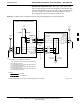
Troubleshooting: Span Control Link 68P09255A69-3 Figure 6-5: MGLI/GLI Board MMI Connection Detail STATUS LED STATUS RESET ALARM SPANS MASTER MMI ACTIVE To MMI port RESET Pushbutton ALARM LED SPANS LED MASTER LED MMI Port Connector ACTIVE LED 8-PIN NULL MODEM BOARD (TRN9666A) 8-PIN TO 10-PIN RS-232 CABLE (P/N 30-09786R01) 6 LMF COMPUTER RS-232 CABLE COM1 OR COM2 6-36 DB9-TO-DB25 ADAPTER 1X SC 4812ET Lite BTS Optimization/ATP Software Release 2.16.1.
Troubleshooting: Span Control Link 68P09255A69-3 Set BTS Site Span Configuration NOTE Perform the following procedure ONLY if span configurations loaded in the MGLI2/GLI2s do not match those in the OMCR/CBSC data base, AND ONLY when the exact configuration data is available. Loading incorrect span configuration data will render the site inoperable.
Troubleshooting: Span Control Link 68P09255A69-3 Table 6-32: Set BTS Span Parameter Configuration Step 6 Action If the current MGLI/GLI span rate must be changed, enter the following MMI command: config ni linkspeed The terminal will display a response similar to the following: Next available options: LIST - linkspeed : Span Linkspeed 56K : 56K (default for T1_1 and T1_3 systems) 64K : 64K (default for all other span configurations) > NOTE With this command, all active (in-use) spans will be se
Troubleshooting: Span Control Link 68P09255A69-3 Table 6-32: Set BTS Span Parameter Configuration Step 10 Action At the entry prompt (>), enter the designator from the list for the span to be changed as shown in the following example: > a The terminal will display a response similar to the following: COMMAND SYNTAX: config ni equal a equal Next available options: LIST equal : Span Equalization 0 : 0-131 feet (default for T1/J1) 1 : 132-262 feet 2 : 263-393 feet 3 : 394-524 feet 4 : 525-655 feet
Troubleshooting: Span Control Link 68P09255A69-3 Table 6-32: Set BTS Span Parameter Configuration Step 14 Action Once the MGLI/GLI has reset, execute the following command to verify span settings are as required: config ni current (equivalent of span view command) The system will respond with a display similar to the following: The frame format in flash Equalization: Span A - 0-131 feet Span B - 0-131 feet Span C - Default (0-131 Span D - Default (0-131 Span E - Default (0-131 Span F - Default (0-
A Appendix A Data Sheets Aug 2002 1X SC 4812ET Lite BTS Optimization/ATP Software Release 2.16.1.
Optimization (Pre-ATP) Data Sheets A 68P09255A69-3 Optimization (Pre-ATP) Data Sheets Verification of Test Equipment Used Table A-1: Verification of Test Equipment Used Manufacturer Model Serial Number Comments:________________________________________________________ __________________________________________________________________ A-2 1X SC 4812ET Lite BTS Optimization/ATP Software Release 2.16.1.
Optimization (Pre-ATP) Data Sheets 68P09255A69-3 A Site Checklist Table A-2: Site Checklist OK Parameter Specification Deliveries Per established procedures Floor Plan Verified Inter Frame Cables: Ethernet Frame Ground Power Per procedure Per procedure Per procedure Factory Data: BBX Test Panel RFDS Per procedure Per procedure Per procedure Site Temperature Dress Covers/Brackets Comments Preliminary Operations Table A-3: Preliminary Operations OK Parameter Specif
Optimization (Pre-ATP) Data Sheets A 68P09255A69-3 Pre-Power and Initial Power Tests Table A3a: Pre-power Checklist OK Parameter Specification Pre-power-up tests Table 2-3 Table 2-4 Internal Cables: Span CSM Power Ethernet Connectors LAN A ohms LAN B ohms LAN A shield LAN B shield LAN A IN & OUT terminators LAN B IN & OUT terminators Ethernet Boots Air Impedance Cage (single cage) installed Initial power-up tests Table 2-4 Table 2-6 Table 2-7 Frame fans LEDs operatio
Optimization (Pre-ATP) Data Sheets 68P09255A69-3 A General Optimization Checklist Table A3b: General Optimization Checklist OK Parameter Specification Preparing the LMF Load LMF software Create site-specific BTS directory Create HyperTerminal connection Table 3-1 Table 3-2 Table 3-4 LMF-to-BTS Connection Verify GLI2 ethernet address settings Ping LAN A Ping LAN B Table 3-10 Table 6-3 Table 3-16 Table 3-16 Table 3-17 Verify ROM code loads for software release Do
Optimization (Pre-ATP) Data Sheets A 68P09255A69-3 GPS Receiver Operation Table A-4: GPS Receiver Operation OK Parameter Specification GPS Receiver Control Task State: tracking satellites Verify parameter Initial Position Accuracy: Verify Estimated or Surveyed Current Position: lat lon height RECORD in msec and cm also convert to deg min sec Current Position: satellites tracked Estimated: (>4) satellites tracked,(>4) satellites visible Surveyed: (>1) satellite tracked,(>4) satellites
Optimization (Pre-ATP) Data Sheets 68P09255A69-3 A LFR Receiver Operation Table A-5: LFR Receiver Operation OK Parameter Specification Station call letters M X Y Z assignment.
Optimization (Pre-ATP) Data Sheets A 68P09255A69-3 LPA IM Reduction Table A-6: LPA IM Reduction Parameter OK Comments CARRIER LPA # 2:1 3-Sector BP 3-Sector Specification 1A C1 C1 No Alarms 1B C1 C1 No Alarms 1C C1 C1 No Alarms 1D C1 C1 No Alarms 3A C2 C2 No Alarms 3B C2 C2 No Alarms 3C C2 C2 No Alarms 3D C2 C2 No Alarms Comments:_________________________________________________________ A-8 1X SC 4812ET Lite BTS Optimization/ATP Software Rele
Optimization (Pre-ATP) Data Sheets 68P09255A69-3 TX Bay Level Offset / Power Output Verification for 3-Sector Configurations 1-Carrier 2-Carrier Non-adjacent Channels Table A-7: TX BLO Calibration (3-Sector: 1-Carrier and 2-Carrier Non-adjacent Channels) OK Parameter Specification Comments BBX2-1, ANT-1A = BBX2-r , ANT-1A = dB dB BBX2-2, ANT-2A = BBX2-r , ANT-2A = dB dB BBX2-3, ANT-3A = BBX2-r , ANT-3A = dB dB BBX2-4, ANT-1B = BBX2-r , ANT-1B = dB dB BBX2-5, ANT-2B = BBX2-r , ANT-2B = dB
Optimization (Pre-ATP) Data Sheets A 68P09255A69-3 2-Carrier Adjacent Channel Table A-8: TX Bay Level Offset Calibration (3-Sector: 2-Carrier Adjacent Channels) OK Parameter Specification Comments BBX2-1, ANT-1A = BBX2-r , ANT-1A = dB dB BBX2-2, ANT-2A = BBX2-r , ANT-2A = dB dB BBX2-3, ANT-3A = BBX2-r , ANT-3A = dB dB BBX2-4, ANT-1B = BBX2-r , ANT-1B = dB dB BBX2-5, ANT-2B = BBX2-r , ANT-2B = dB dB BBX2-6, ANT-3B = BBX2-r , ANT-3B = dB dB BBX2-1, ANT-1A = BBX2-r , ANT-1A = dB d
Optimization (Pre-ATP) Data Sheets 68P09255A69-3 A Table A-9: TX Antenna VSWR OK Parameter Specification VSWR Antenna 3A < (1.5 : 1) VSWR Antenna 1B < (1.5 : 1) VSWR Antenna 2B < (1.5 : 1) VSWR Antenna 3B < (1.5 : 1) Data Comments:________________________________________________________ __________________________________________________________________ Aug 2002 1X SC 4812ET Lite BTS Optimization/ATP Software Release 2.16.1.
Optimization (Pre-ATP) Data Sheets A 68P09255A69-3 RX Antenna VSWR Table A-10: RX Antenna VSWR OK Parameter Specification VSWR Antenna 1A < (1.5 : 1) VSWR Antenna 2A < (1.5 : 1) VSWR Antenna 3A < (1.5 : 1) VSWR Antenna 1B < (1.5 : 1) VSWR Antenna 2B < (1.5 : 1) VSWR Antenna 3B < (1.
Site Serial Number Check List 68P09255A69-3 A Site Serial Number Check List Date Site SCCP Shelf NOTE: For BBXs and MCCs, enter the type as well as serial number; for example, BBX2, BBX-1X, MCC8, MCC24, MCC-1X. Site I/O A & B SCCP Shelf CSM-1 CSM-2 HSO/LFR CCD-1 CCD-2 AMR-1 AMR-2 MPC-1 MPC-2 Fans 1-2 GLI2-1 GLI2-2 BBX-1 BBX-2 BBX-3 BBX-4 BBX-5 BBX-6 BBX-R1 MCC-1 MCC-2 MCC-3 MCC-4 CIO SWITCH PS-1 PS-2 Aug 2002 1X SC 4812ET Lite BTS Optimization/ATP Software Release 2.16.1.
Site Serial Number Check List A 68P09255A69-3 LPAs LPA 1A LPA 1B LPA 1C LPA 1D LPA 3A LPA 3B LPA 3C LPA 3D A-14 1X SC 4812ET Lite BTS Optimization/ATP Software Release 2.16.1.
B Appendix B FRU Optimization/ATP Test Matrix Aug 2002 1X SC 4812ET Lite BTS Optimization/ATP Software Release 2.16.1.
FRU Optimization/ATP Test Matrix 68P09255A69-3 FRU Optimization/ATP Test Matrix Usage & Background Periodic maintenance of a site may also mandate re-optimization of specific portions of the site. An outline of some basic guidelines is included in the following tables. B NOTE Re-optimization steps listed for any assembly detailed in the tables below must be performed anytime an RF cable associated with it is replaced.
FRU Optimization/ATP Test Matrix 68P09255A69-3 Table 3-41 TX Path Calibration 4 Table 3-42 Download Offsets to BBX 4 Table 3-43 TX Path Audit 4 Table 3-51 RFDS Path Calibration and Offset Data Download 6 Table 4-8 Spectral Purity TX Mask 4 Table 4-9 Waveform Quality (rho) 4 Table 4-10 Pilot Time Offset 4 Table 4-11 Code Domain Power / Noise Floor 4 Table 4-12 FER Test 5 Table 3-54 through Table 3-63 Alarm Tests 4 1 4 5 5 4 5 5 9 9 1 4
FRU Optimization/ATP Test Matrix 68P09255A69-3 RFDS Switch Card RFDS Cables LPA Bandpass Filter or Combiner LPA or LPA Trunking Module LPAC Cable ETIB or Associated Cables GLI2 CCD Card RGD/20-pair Punchblock with RGD 50-pair Punchblock (with RGPS) HSO/HSOX LFR CSM/GPS MCC24E/MCC8E/MCC-1X BBX2/BBX-1X MPC / EMPC CIO TX Cables Description RX Cables Doc Tbl # DRDC or TRDC B SCCP Shelf Assembly (Backplane) Table B-1: SC 4812ET Lite BTS Optimization and ATP Test Matrix OPTIMIZATION AN
C Appendix C BBX Gain Set Point vs. BTS Output Aug 2002 1X SC 4812ET Lite BTS Optimization/ATP Software Release 2.16.1.
BBX Gain Set Point vs. BTS Output 68P09255A69-3 BBX Gain Set Point vs. BTS Output Usage & Background Table C-1 outlines the relationship between the total of all code domain channel element gain settings (digital root sum of the squares) and the BBX Gain Set Point between 33.0 dBm and 44.0 dBm. The resultant RF output (as measured in dBm at the BTS antenna connector) is shown in the table. The table assumes that the BBX Bay Level Offset (BLO) values have been calculated.
BBX Gain Set Point vs. BTS Output 68P09255A69-3 Table C-1: BBX Gain Set Point vs. Actual BTS Output (in dBm) 44 43 42 41 40 39 38 37 36 35 34 33 381 - - - - 43.3 42.3 41.3 40.3 39.3 38.3 37.3 36.3 374 - - - - 43.1 42.1 41.1 40.1 39.1 38.1 37.1 36.1 366 - - - - 42.9 41.9 40.9 39.9 38.9 37.9 36.9 35.9 358 - - - - 42.7 41.7 40.7 39.7 38.7 37.7 36.7 35.7 350 - - - 43.5 42.5 41.5 40.5 39.5 38.5 37.5 36.5 35.5 342 - - - 43.3 42.
BBX Gain Set Point vs. BTS Output 68P09255A69-3 Notes C C-4 1X SC 4812ET Lite BTS Optimization/ATP Software Release 2.16.1.
Appendix D D CDMA Operating Frequency Information Aug 2002 1X SC 4812ET Lite BTS Optimization/ATP Software Release 2.16.1.
CDMA Operating Frequency Programming Information 68P09255A69-3 CDMA Operating Frequency Programming Information Introduction Programming of each of the BTS BBX synthesizers is performed by the BTS GLI2s via the Concentration Highway Interface (CHI) bus. This programming data determines the transmit and receive transceiver operating frequencies (channels) for each BBX. 1900 MHz PCS Channels Figure D-1 shows the valid channels for the North American PCS 1900 MHz frequency spectrum.