Optimization/Calibration – Introduction – continued antenna feed line loss can be combined to determine the required power at the frame antenna connections. The corresponding BBX2 output level required to achieve that power level on any channel/sector can then be determined based on Bay Level Offset (BLO) data determined during the optimization process.
Preparing the LMF Overview Before optimization can be performed, the CDMA LMF must be installed and configured on a computer platform meeting Motorola–specified requirements (see Recommended Test Equipment and Software in Chapter 1). IMPORTANT * 3 For the CDMA LMF graphics to display properly, the computer platform must be configured to display more than 256 colors. See the operating system software instructions for verifying and configuring the display settings.
Preparing the LMF – continued Table 3-1: CD ROM Installation n Step Action 3 Select Run. 4 Enter d:\autorun in the Open box and click OK. NOTE (If applicable, replace the letter d with the correct CD ROM drive letter.) 5 3 Follow the directions displayed in the Setup screen. Copy CBSC CDF Files to the LMF Computer Before logging on to a BTS with the CDMA LMF computer to execute optimization/ATP procedures, the correct bts-#.cdf and cbsc-#.
Preparing the LMF – continued Table 3-2: Copying CBSC CDF Files to the LMF Computer Step 4 Action Type mount and press the Enter key. NOTE S Look for the “floppy/no_name” message on the last line displayed. S If the eject command was previously entered, floppy/no_name will be appended with a number. Use the explicit floppy/no_name reference displayed when performing step 7. 3 5 Change to the directory, where the files to be copied reside, by typing cd (e.g.
Preparing the LMF – continued Creating a Named HyperTerminal Connection for MMI Communication Confirming or changing the configuration data of certain BTS Field Replaceable Units (FRU) requires establishing an MMI communication session between the CDMA LMF computer and the FRU. Using features of the Windows operating system, the connection properties for an MMI session can be saved on the CDMA LMF computer as a named Windows HyperTerminal connection.
Preparing the LMF – continued Table 3-3: Create HyperTerminal Connection Step 5 Action In the Port Settings tab of the COM# Properties window displayed, configure the RS–232 port settings as follows: S S S S S 3 Bits per second: 9600 Data bits: 8 Parity: None Stop bits: 1 Flow control: None 6 Click OK. 7 Save the defined connection by selecting: File > Save 8 Close the HyperTerminal window by selecting: File > Exit 9 Click the Yes button to disconnect when prompted.
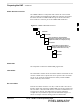
Preparing the LMF – continued Folder Structure Overview The CDMA LMF uses a wlmf folder that contains all of the essential data for installing and maintaining the BTS. The following list outlines the folder structure for CDMA LMF. Except for the bts-nnn folders, these folders are created as part of the CDMA LMF installation.
Preparing the LMF – continued Figure 3-2: BTS Folder Name Syntax Example bts–259 BTS Number 3 bts–nnn.cal File The CAL (Calibration) file contains the bay level offset data (BLO) that is used for BLO downloads to the BBX devices. The CAL file is automatically created and updated by the CDMA LMF when TX calibration is performed. Figure 3-3 details the file name syntax for the CAL file. Figure 3-3: CAL File Name Syntax Example bts–259.cal BTS Number bts–nnn.
Preparing the LMF – continued cbsc File The cbsc–#.cdf (Centralized Base Station Controller) file contains data for the BTS. If one is not obtained from the CBSC, a copy of the default cbsc–1.cdf file located in the cdma folder can be used. IMPORTANT * Using the generic cbsc–1.cdf file will not provide a valid optimization unless the generic file is edited to replace default parameters with local operational parameters (e.g.
Preparing the LMF – continued Figure 3-5: Code Load File Name Syntax Example bbx_ram.bin.0600 Device Type Hardware bin number If this number matches the bin number of the device, the code file will automatically be used for the download* 3 * The device bin number can be determined by using the Status function after logging into a BTS. If the device does not have a bin number, one of the following default numbers must be used.
Preparing the LMF – continued Figure 3-6: DDS File Name Syntax Example csm.dds.0800 Device Type Device Bin Type Number If this number matches the bin number of the device, the DDS file will automatically be used for the download* 3 * The device bin number can be determined by using the Status function after logging into a BTS. If the device does not have a bin number, one of the following default numbers must be used.
Span Lines – Interface and Isolation T1/E1 Span Interface IMPORTANT * At active sites, the OMC–R/CBSC must disable the BTS and place it out of service (OOS). DO NOT remove the span line cable conectors until the OMC–R/CBSC has disabled the BTS. Each frame is equipped with one 50–pair punchblock for spans, customer alarms, remote GPS, and BTS frame alarms. See Figure 3-9 and refer to Table 3-5 for the physical location and punchdown location information.
Span Lines – Interface and Isolation – continued T1/E1 Span Isolation Table 3-4 describes the action required for span isolation. Table 3-4: T1/E1 Span Isolation Step Action 1 Have the OMCR/CBSC place the BTS OOS. 2 To disable the span lines, locate the connector for the span or spans which must be disabled and remove the respective connector from the applicable SCCP cage Span I/O board (Figure 3-7).
Span Lines – Interface and Isolation – continued S A PC using the AT 9–pin interface S A modem using the 9–pin connector S Other shelves in a daisy chain Figure 3-8: Rear and Front View of CSU Shelf 3 To/From Network To/From GLI2 To/From Network To/From GLI2 Rear View SLOT 1 SLOT 2 DCE Connector (Craft Port) CSU Modules REF.
Span Lines – Interface and Isolation – continued Alarm and Span Line Cable Pin/Signal Information See Figure 3-9 and refer to Table 3-5 for the physical location and punchdown location information for the 50–pair punchblock.
Span Lines – Interface and Isolation – continued Table 3-5: Punchdown Location for 50–Pair Punch Block Site Component Signal Name NOT USED 3 LFR/HSO PILOT BEACON CUSTOMER OUTPUTS / INPUTS LFR_HSO_GND EXT_IPPS_POS EXT_IPPS_NEG CAL_+ CAL_– LORAN_ + LORAN_ – Pilot Beacon Alarm – Minor Pilot Beacon Alarm – Rtn Pilot Beacon Alarm – Major Pilot Beacon Control – NO Pilot Beacon Control–COM Pilot Beacon Control – NC Customer Outputs 1 – NO Customer Outputs 1 – COM Customer Outputs 1 – NC Customer Outputs 2
Span Lines – Interface and Isolation – continued Table 3-5: Punchdown Location for 50–Pair Punch Block Site Component CUSTOMER OUTPUTS / INPUTS SPAN RGPS Phone Line Miscellaneous 08/01/2001 Signal Name Cust_Rtn_A_8 Customer Inputs 9 Cust_Rtn_A_9 Customer Inputs 10 Cust_Rtn_A_10 RVC_TIP_A RVC_RING_A XMIT_TIP_A XMIT_RING_A RVC_TIP_B RVC_RING_B XMIT_TIP_B XMIT_RING_B RVC_TIP_C RVC_RING_C XMIT_TIP_C XMIT_RING_C RVC_TIP_D RVC_RING_D XMIT_TIP_D XMIT_RING_D RVC_TIP_E RVC_RING_E XMIT_TIP_E XMIT_RING_E RVC_TI
LMF to BTS Connection LMF to BTS Connection The CDMA LMF computer may be connected to the LAN A or B connector located behind the frame lower air intake grill. Figure 3-10 below shows the general location of these connectors. LAN A is considered the primary LAN. Table 3-6: Connect the LMF to the BTS 3 Step Action 1 To gain access to the LAN connectors, open the LAN cable and utility shelf access panel, then pull apart the hook–and–loop fabric covering the BNC “T” connector (see Figure 3-10).
Using CDMA LMF Basic CDMA LMF Operation The CDMA LMF allows the user to work in the two following operating environments which are accessed using the specified desktop icons: S Graphical User Interface (GUI) using the WinLMF icon S Command Line Interface (CLI) using the WinLMF CLI icon The GUI is the primary optimization and acceptance testing operating environment.
Using CDMA LMF – continued separate FRAME tab for each frame(for example, FRAME–438–1, and FRAME–438–101 for BTS–438 that has both frames). If an RFDS is included in the CDF file, an RFDS tab (e.g., RFDS–438–1) will be displayed. Actions, such as ATP tests, can be initiated for selected devices in one or more frames of a logical BTS. Refer to the CDMA LMF Select devices help screen for information on how to select devices. 3 Logging Into a BTS CAUTION Be sure that the correct bts–#.cdf and cbsc–#.
Using CDMA LMF – continued BTS Login from the GUI Environment Follow the procedures in Table 3-7 to log into a BTS when using the GUI environment. Table 3-7: BTS GUI Login Procedure n Step 1 Action Start the CDMA LMF GUI environment by double–clicking on the WinLMF desktop icon (if the LMF is not running). NOTE If a warning similar to the following is displayed, select No, shut down other LMF sessions which may be running, and start the CDMA LMF GUI environment again: The CLI handler is already running.
Using CDMA LMF – continued BTS Login from the CLI Environment Follow the procedures in Table 3-8 to log into a BTS when using the CLI environment. IMPORTANT * 3 If the CLI and GUI environments are to be used at the same time, the GUI must be started first and BTS login must be performed from the GUI. Refer to Table 3-7 to start the GUI environment and log into a BTS.
Using CDMA LMF – continued IMPORTANT * The GUI and CLI environments use the same connection to a BTS. If a BTS is logged into in both the GUI and CLI environments at the same time, logging out of the BTS in either environment will log out of it for both. When either a login or logout is performed in the CLI window, there is no GUI indication that the login or logout has occurred.
Using CDMA LMF – continued Logging Out of a BTS from the CLI Environment Follow the procedure in Table 3-10 to logout of a BTS when using the CLI environment. Table 3-10: BTS CLI Logout Procedure n Step Action * IMPORTANT If the BTS is also logged into from a GUI running at the same time and further work must be done with it in the GUI, proceed to step 2. 3 1 Logout of a BTS by entering the following command: logout bts– A response similar to the following will be displayed: LMF> 13:24:51.
Using CDMA LMF – continued Table 3-11: Establishing MMI Communication Step Action NOTE If a Windows desktop shortcut was not created for the MMI connection, access the connection from the Windows Start menu by selecting: Programs > Accessories > Hyperterminal > HyperTerminal >
Pinging the Processors Pinging the BTS For proper operation, the integrity of the Ethernet LAN A and B links must be be verified. Figure 3-12 represents a typical BTS Ethernet configuration for the SC4812ET Lite with an expansion frame. The drawing depicts cabling and termination for both the A and B LANs. Ping is a program that sends request packets to the LAN network modules to get a response from the specified “target” module.
Pinging the Processors – continued IMPORTANT * The Ethernet LAN A and B cables and/or terminations must be installed on each frame/enclosure external LAN connector before performing this test. All other processor board LAN connections are made through the backplanes. Table 3-12: Pinging the Processors 3 Step Action 1 If this is a first–time communication with a newly–installed frame or a GLI2 which has been replaced, perform the procedure in Table 6-3 and then return to step 2.
Pinging the Processors – continued Table 3-12: Pinging the Processors Step Action 13 If ping was unsuccessful after restarting the CDMA LMF computer, press the MGLI front panel reset pushbutton and perform steps 6 through 9 again. 14 NOTE Refer to Table 6-1 if ping was unsuccessful after resetting the MGLI. 3 15 After the BTS has been successfully pinged, be sure the 50Ω termination was replaced on the BTS frame LAN B IN connector in the power entry compartment (Figure 3-12).
Download the BTS Overview Before a BTS can operate, each equipped device must contain device initialization (ROM) code. ROM code is loaded in all devices during manufacture or factory repair. Device application (RAM) code and data must be downloaded to each equipped device by the user before the BTS can be made fully functional for the site where it is installed. ROM Code 3 Downloading ROM code to BTS devices from the CDMA LMF is NOT routine maintenance or a normal part of the optimization process.
Download the BTS – continued RAM code downloading requires a few minutes. After the download starts, the non–GLI device being loaded changes to OOS–ROM (blue). If the download is completed successfully, the non–GLI device changes to OOS–RAM (yellow).
Download the BTS – continued Download RAM Code and Data to MGLI and GLI Follow the steps outlined in Table 3-14 to download the RAM code and data to the MGLI and other installed GLI devices. Prerequisites S Prior to performing these procedures, ensure a code file exists for each of the devices to be loaded. S The CDMA LMF computer is connected to the BTS (refer to 3 Table 3-6), and is logged in using the GUI environment (refer to Table 3-7).
Download the BTS – continued Table 3-15: Download RAM Code and Data to Non–GLI Devices Step Action 1 Select the target CSM, MCC, and BBX device(s). 2 From the Device pull down menu, select Download Code. A status report is displayed that shows the results of the download for each selected device. Click OK to close the status report window when downloading is completed.
Download the BTS – continued Table 3-16: Select CSM Clock Source Step 6 7 Action Click on the OK button. A status report window is displayed showing the results of the selection action. Click on the OK button to close the status report window. 3 Enable CSMs Each BTS CSM system features two CSM boards per site. In a typical operation, the primary CSM locks its Digital Phase Locked Loop (DPLL) circuits to GPS signals.
Download the BTS – continued Table 3-17: Enable CSMs Step Action * IMPORTANT The GPS satellite system satellites are not in a geosynchronous orbit and are maintained and operated by the United States Department of Defense (DOD). The DOD periodically alters satellite orbits; therefore, satellite trajectories are subject to change. A GPS receiver that is INS contains an “almanac” that is updated periodically to take these changes into account.
CSM System Time – GPS & LFR/HSO Verification Clock Synchronization Manager (CSM) System Time The primary function of the Clock Synchronization Manager (CSM) cards is to maintain CDMA system time. The CSM card in SCCP shelf slot CSM–1 is the primary timing source while the card in slot CSM–2 provides redundancy. The second generation CSM card (CSM2) is required when using the remote GPS receiver (R–GPS). R–GPS uses a GPS receiver in the antenna head that has a digital output to the CSM2 card.
CSM System Time – GPS & LFR/HSO Verification – continued synchronized to Universal Time Coordinates (UTC) and GPS time. The LFR can maintain system time indefinately after initial GPS lock. The HSO is a high stability 10 MHz oscillator with the necessary interface to the CSMs. The HSO is typically installed in those geographical areas not covered by the LORAN–C system. Since the HSO is a free–standing oscillator, system time can only be maintained for 24 hours after 24 hours of GPS lock.
CSM System Time – GPS & LFR/HSO Verification – continued CSM Frequency Verification The objective of this procedure is the initial verification of the Clock Synchronization Module (CSM) cards before performing the RF path verification tests. Test Equipment Setup (GPS & LFR/HSO Verification) Follow the steps outlined in Table 3-19 to set up test equipment.
CSM System Time – GPS & LFR/HSO Verification – continued Figure 3-13: CSM MMI Terminal Connection REFERENCE OSCILLATOR CSM card shown removed from frame MMI SERIAL PORT 3 EVEN SECOND TICK TEST POINT REFERENCE GPS RECEIVER ANTENNA INPUT ANTENNA COAX CABLE GPS RECEIVER 19.6 MHZ TEST POINT REFERENCE (NOTE 1) NULL MODEM BOARD (TRN9666A) 9–PIN TO 9–PIN RS–232 CABLE FW00372 LMF NOTEBOOK DB9–TO–DB25 ADAPTER RS–232 SERIAL MODEM CABLE COM1 NOTES: 1.
CSM System Time – GPS & LFR/HSO Verification – continued Table 3-20: GPS Initialization/Verification Step Action 1 To verify that Clock alarms (0000), Dpll is locked and has a reference source, and GPS self test passed messages are displayed within the report, issue the following MMI command bstatus – The system will display a response similiar to the following: 3 CSM Status INS:ACTIVE Slot A Clock MASTER.
CSM System Time – GPS & LFR/HSO Verification – continued Table 3-20: GPS Initialization/Verification Step Action 3 HSO information (underlined text above, verified from left to right) is usually the #1 reference source. If this is not the case, have the OMCR determine the correct BTS timing source has been identified in the database by entering the display bts csmgen command and correct as required using the edit csm csmgen refsrc command.
CSM System Time – GPS & LFR/HSO Verification – continued Table 3-20: GPS Initialization/Verification Step 5 Action Enter the following command at the CSM> prompt to verify that the GPS receiver is in tracking mode.
CSM System Time – GPS & LFR/HSO Verification – continued Table 3-20: GPS Initialization/Verification Step 7 Action If steps 1 through 6 pass, the GPS is good. * IMPORTANT If any of the above mentioned areas fail, verify that: – If Initial position accuracy is “estimated” (typical), at least 4 satellites must be tracked and visible (1 satellite must be tracked and visible if actual lat, log, and height data for this site has been entered into CDF file).
CSM System Time – GPS & LFR/HSO Verification – continued LORAN–C Initialization/Verification Table 3-21: LORAN–C Initialization/Verification Step Action 1 At the CSM> prompt, enter lstatus to verify that the LFR is in tracking mode.
CSM System Time – GPS & LFR/HSO Verification – continued Table 3-21: LORAN–C Initialization/Verification Step Action Note 2 Verify the following LFR information (highlighted above in boldface type): – Locate the “dot” that indicates the current phase locked station assignment (assigned by MM). – Verify that the station call letters are as specified in site documentation as well as M X Y Z assignment. – Verify the S/N ratio of the phase locked station is greater than 8.
Test Equipment Setup Connecting Test Equipment to the BTS All test equipment is controlled by the LMF through an IEEE–488/GPIB bus. The LMF requires each piece of test equipment to have a factory set GPIB address.
Test Equipment Set–up – continued Test Equipment Preparation For specific steps to prepare each type of test set and power meter to perform calibration and ATP, see Appendix F. Test Equipment Connection Chart Table 3-22 depicts the current test equipment available meeting Motorola standards. 3 To identify the connection ports, locate the test equipment presently being used in the TEST SETS columns, and read down the column.
Test Equipment Set–up – continued Equipment Warm-up IMPORTANT * Warm-up BTS equipment for a minimum of 60 minutes prior to performing the BTS optimization procedure. This assures BTS site stability and contributes to optimization accuracy. (Time spent running initial power-up, hardware/firmware audit, and BTS download counts as warm-up time.) WARNING Before installing any test equipment directly to any BTS TX OUT connector, verify there are no CDMA BBX channels keyed.
Test Equipment Set–up – continued Figure 3-14: Cable Calibration Test Setup SUPPORTED TEST SETS CALIBRATION SET UP Motorola CyberTest A. SHORT CABLE CAL ÏÏÏ ÏÏÏÌ 3 ANT IN SHORT CABLE TEST SET RF GEN OUT Note: The Directional Coupler is not used with the Cybertest Test Set. The TX cable is connected directly to the Cybertest Test Set. B. RX TEST SETUP A 10dB attenuator must be used with the short test cable for cable calibration with the CyberTest Test Set.
Test Equipment Set–up – continued Manual Cable Calibration If manual cable calibration is required, refer to the procedures in Appendix F. Set–up for TX Calibration Figure 3-15 and Figure 3-16 show the test set connections for TX calibration. Figure 3-15: TX Calibration Test Setup (CyberTest and HP 8935) 3 TEST SETS TRANSMIT (TX) SET UP Motorola CyberTest POWER SENSOR ÏÏÏ ÏÏÏÌ Ì FRONT PANEL POWER METER (OPTIONAL)* 100–WATT (MIN) NON–RADIATING RF LOAD OUT DIRECTIONAL COUPLER (30 DB) 50 Ω ΤERM.
Test Equipment Set–up – continued Figure 3-16: TX Calibration Test Setup HP 8921A and Advantest TEST SETS TRANSMIT (TX) SET UP NOTE: THE HP8921A AND ADVANTEST CANNOT BE USED FOR TX CALIBRATION. A POWER METER MUST BE USED. 100–WATT (MIN) NON–RADIATING RF LOAD POWER SENSOR POWER METER 3 DIRECTIONAL COUPLER (30 DB) 50 Ω ΤERM.
Test Equipment Set–up – continued Setup for Optimization/ATP Figure 3-17 and Figure 3-18 show the test set connections for optimization/ATP tests. Figure 3-17: Optimization/ATP Test Setup Calibration (CyberTest, HP 8935 and Advantest) TEST SETS Optimization/ATP SET UP Motorola CyberTest SYNC MONITOR EVEN SEC TICK PULSE REFERENCE FROM CSM BOARD FREQ MONITOR 19.
Test Equipment Set–up – continued Figure 3-18: Optimization/ATP Test Setup HP 8921A TEST SETS Optimization/ATP SET UP Hewlett–Packard Model HP 8921A W/PCS Interface (for 1700 and 1900 MHz) SYNC MONITOR EVEN SEC TICK PULSE REFERENCE FROM CSM BOARD FREQ MONITOR 19.6608 MHZ CLOCK REFERENCE FROM CSM BOARD NOTE: IF BTS RX/TX SIGNALS ARE DUPLEXED, BOTH THE TX AND RX TEST CABLES CONNECT TO THE DUPLEXED ANTENNA GROUP AND USE THE 30 DB DIRECTIONAL COUPLER AND 20 DB IN–LINE ATTENUATOR.
Test Set Calibration Background Proper test equipment set–up ensures that all measurements are correct and the test equipment and associated test cables do not introduce measurement errors. NOTE If the test equipment set (see Chapter 1, Terms and Abbreviations) being used to interface with the BTS has been calibrated and maintained as a set, this procedure does not need to be performed. This procedure must be performed before the optimization.
Test Set Calibration – continued Manual cable calibration procedures using the HP8921A and Advantest R3465 communications test sets are provided in Appendix F, if needed. Manual power meter calibration procedures are also included in Appendix F. Selecting Test Equipment Prerequisites A Serial Connection and a Network Connection tab are provided for test equipment selection.
Test Set Calibration – continued Table 3-23: Selecting Test Equipment Manually in a Serial Connection Tab Step 7 Action Click on Apply. (The button will darken until the selection has been recorded.) NOTE With manual selection, CDMA LMF does not detect the test equipment to see if it is connected and communicating with CDMA LMF. 8 Click on Dismiss to close the test equipment window.
Test Set Calibration – continued Calibrating Test Equipment The calibrate test equipment function zeros the power measurement level of the test equipment item that is to be used for TX calibration and audit. If both a power meter and an analyzer are connected (for example, an HP 437 and an HP8921A/600), only the power meter is zeroed. Calibrate Test Equipment from the Util menu list is used to calibrate test equipment item before being used for testing.
Test Set Calibration – continued of the TX cable configuration must be as required for the BTS (normally 30 or 50 dB). The Motorola Cybertest analyzer is different in that the required attenuation/load is built into the test set so the TX cable configuration consists only of the required length coax cable. Calibrating Cables with a CDMA Analyzer The Cable Calibration menu item from the Util menu list is used to calibrate both TX and RX test cables for use with CDMA LMF.
Test Set Calibration – continued Calibrating TX Cables Using a Signal Generator and Spectrum Analyzer Follow the procedure in Table 3-27 to calibrate the TX cables using the signal generator and spectrum analyzer. Refer to Figure 3-19 for a diagram of the signal generator and spectrum analyzer. Table 3-27: Calibrating TX Cables Using Signal Generator and Spectrum Analyzer 3 Step Action 1 Connect a short test cable between the spectrum analyzer and the signal generator.
Test Set Calibration – continued Calibrating RX Cables Using a Signal Generator and Spectrum Analyzer Follow the procedure in Table 3-28 to calibrate the RX cables using the signal generator and spectrum analyzer. Refer to Figure 3-20, if required. Table 3-28: Calibrating RX Cables Using a Signal Generator and Spectrum Analyzer Step Action 1 Connect a short test cable to the spectrum analyzer and connect the other end to the Signal Generator.
Test Set Calibration – continued Setting Cable Loss Values Cable loss values for the TX and RX test cable configurations are normally set by accomplishing automatic cable calibration with use of the applicable test equipment. The resulting values are stored in the cable loss files. The cable loss values can also be set/changed manually. CAUTION Cable loss values must be manually entered in the LMF database if manual cable calibration was performed.
Test Set Calibration – continued Setting TX Coupler Loss Value If an in–service TX coupler is installed the coupler loss (e.g., 30 dB) must be manually entered so it will be included in the LMF TX calibration and audit calculations. Prerequisites S Logged into the BTS Table 3-30: Setting TX Coupler Loss Values Step Action 1 Click on the Util menu. 2 Select Edit > TX Coupler Loss. A data entry pop–up window will appear.
Bay Level Offset Calibration Introduction Calibration compensates for normal equipment variations within the BTS and assures maximum measurement accuracy. RF Path Bay Level Offset Calibration Bay Level Offset (BLO) calibration identifies the accumulated gain in every transmit path (BBX2 slot) at the BTS site and stores that value in the CDMA LMF CAL file. The BLOs are subsequently downloaded to each BBX2.
Bay Level Offset Calibration – continued TX Path Calibration The TX Path Calibration assures correct site installation, cabling, and the first order functionality of all installed equipment. The proper function of each RF path is verified during calibration. The external test equipment is used to validate/calibrate the TX paths of the BTS. WARNING Before installing any test equipment directly to any TX OUT connector you must first verify that there are no CDMA channels keyed.
Bay Level Offset Calibration – continued BLO Calibration Data File During the calibration process, the CDMA LMF creates a calibration (CAL) data file where BLO values are stored. After calibration has been completed, this offset data must be downloaded to the BBX2s using the CDMA LMF Download BLO function. An explanation of the file is shown below. NOTE 3 Due to the size of the file, Motorola recommends printing out a copy of a bts.cal file and referring to it for the following descriptions.
Bay Level Offset Calibration – continued S The second breakdown of the array is by BBX by sector. Three sectors are allowed. Table 3-32: SC4812ET Lite BTS.cal File Array (Per Sector) BBX2 Sectorization TX Branch RX Branch RX Diversity Branch Slot[1] (Primary BBX2s 1 through 6) 1 (Omni) 2 3–Sector, 1st Carrier 3 4 5 3–Sector, 2nd Carrier 6 Not Used in SC4812ET Lite (CAL file entries are Channel 0 with default power set level.
Bay Level Offset Calibration – continued (2500 corresponds to –125 dBm and 27500 corresponds to +125 dBm). S The 10 calibration points for each slot/branch combination must be stored in order of increasing frequency. If less than 10 points (frequencies) are calibrated, the BLO data for the highest frequency calibrated is written into the remainder of the 10 points for that slot/branch.
Bay Level Offset Calibration – continued Table 3-33: Set Up Test Equipment (RF Path Calibration) Step Action ! CAUTION To prevent damage to the test equipment, all transmit (TX) test connections must be via the 30 dB directional coupler for 800 MHz or via a 30 dB coupler with a 20 dB in–line attenuator for 1900 MHz.
Bay Level Offset Calibration – continued additional items may be installed in the transmit path. The additional change in gain from these items could cause BLO verification failure and, therefore, failure of the entire calibration. In these cases, either the Verify BLO checkbox should be unchecked or the additional path losses should be added into each applicable sector using the Util > Edit > TX Coupler Loss... function.
Bay Level Offset Calibration – continued Table 3-34: All Cal/Audit Path Calibration Step Action 1 Configure test equipment for TX path calibration per Table 3-33. 2 Select the BBX2(s) to be calibrated. 3 From the Tests menu, select All Cal/Audit. 4 5 Select the appropriate carrier(s) displayed in the Channels/Carrier pick list. Press and hold the or key to select multiple items. Type the appropriate channel number in the Carrier n Channels box. 6 Click on OK.
Bay Level Offset Calibration – continued Table 3-35: TX Calibration Test Step 3 Action 5 Enter the appropriate channel number in the Carrier n Channels box. 6 Click OK to display the status report window followed by a Directions pop-up window. 7 Follow the cable connection directions as they are displayed. The test results will be displayed in the status report window. 8 Click OK to close the status report window.
Bay Level Offset Calibration – continued Table 3-36: Download BLO Step Action 1 Select the BBX2(s) to be downloaded. 2 From the Device menu, select Download BLO. A status report window displays the result of the download. NOTE 3 Selected device(s) do not change color when BLO is downloaded. Click OK to close the status report window. Calibration Audit Introduction The BLO calibration audit procedure confirms the successful generation and storage of the BLO calibrations.
Bay Level Offset Calibration – continued TX Audit Test The Tests menu item, TX Audit, performs the TX BLO Audit test for a BBX2(s). All measurements are made through the appropriate TX output connector using the calibrated TX cable setup. Prerequisites Before running this test, the following should be done: 3 S CSM–1,GLI2s, BBX2s have correct code load. S Primary CSM and MGLI2 are INS. S All BBX2s are OOS_RAM. S Test equipment and test cables are calibrated and connected for TX BLO calibration.
Bay Level Offset Calibration – continued Create CAL File The Create Cal File function gets the BLO data from BBXs and creates/updates the CAL file for the BTS. If a CAL file does not exist a new one is created. If a CAL file already exists it is updated. After a BTS has been fully optimized a copy of the CAL file must exist so it can be transferred to the CBSC. If TX calibration has been successfully performed for all BBXs and BLO data has been downloaded, a CAL file will exist.
RFDS Setup and Calibration RFDS Description The optional RFDS is used to perform RF tests of the site from the CBSC or from the LMF. The RFDS contains the following FRUs: S Antenna Select Unit (ASU) S FWT Interface Card (FWTIC) S Subscriber Unit Assembly (SUA) 3 For complete information regarding the RFDS, refer to the CDMA CDMA RFDS Hardware Installation; 68P64113A93, CDMA RFDS User’s Guide; 68P64114A51, and the LMF Help function. RFDS Parameter Settings The bts-#.
RFDS Setup and Calibration – continued Table 3-39: RFDS Parameter Settings Step Action * IMPORTANT Log out of the BTS prior to performing this procedure. 1 Using a text editor, verify the following fields are set correctly in the bts–#.cdf file (1 = GLI based RFDS; 2 = Cobra RFDS). EXAMPLE: RfdsEquip = 2 TsuEquip = 1 MC1Equip = 0 MC2Equip = 0 MC3Equip = 0 MC4Equip = 0 Asu1Equip = 1 Asu2Equip = 0 (1 if system is non-duplexed) TestOrigDN = ’123456789’ NOTE The above is an example of the bts-#.
RFDS Setup and Calibration – continued RFDS TSU NAM Programming The NAM (number assignment module) information needs to be programmed into the TSU before it can receive and process test calls, or be used for any type of RFDS test. The RFDS TSU NAM must be programmed with the appropriate system parameters and phone number during hardware installation. The TSU phone and TSU MSI must be recorded for each BTS used for OMC–R RFDS software configuration.
RFDS Setup and Calibration – continued Valid NAM Ranges Table 3-41 provides the valid NAM field ranges. If any of the fields are missing or out-of–range, the RFDS will error out.
RFDS Setup and Calibration – continued Set Antenna Map Data The antenna map data must be entered manually if an RFDS is installed. Antenna map data does not have to be entered if an RFDS is not installed. The antenna map data is only used for RFDS tests and is required if a RFDS is installed. Prerequisite S Logged into the BTS 3 Table 3-42: Set Antenna Map Data Step Action 1 Click on the Util menu. 2 Select Edit > Antenna Map > TX or RX. A data entry pop–up window will appear.
RFDS Setup and Calibration – continued Set RFDS Configuration Data If an RFDS is installed the RFDS configuration data must be manually entered. Prerequisite S Logged into the BTS IMPORTANT * 3 The entered antenna# index numbers must correspond to the antenna# index numbers used in the antenna maps. Table 3-43: Set RFDS Configuration Data Step Action 1 Click on the Util menu. 2 Select Edit > RFDS Configuration > TX or RX. A data entry pop–up window will appear.
RFDS Setup and Calibration – continued RFDS Calibration The RFDS Calibration option is used to calibrate the RFDS TX and RX paths. For a TX antenna path calibration the BTS XCVR is keyed at a pre–determined power level and the BTS power output level is measured by the RFDS. The power level is then measured at the TX antenna directional coupler by the power measuring test equipment item being used (power meter or analyzer).
RFDS Setup and Calibration – continued Table 3-45: RFDS Calibration Step Action 1 Select the RFDS tab. 2 Click on the RFDS menu. 3 Click on the RFDS Calibration menu item. 4 Select the appropriate direction (TX/RX) in the Direction pick list. 5 Enter the appropriate channel number(s) in the Channels box. Separate the channel numbers with a comma or a dash if more than one channel number is entered (e.g., 247,585,742 or 385–395 for through).
RFDS Setup and Calibration – continued Program TSU NAM Follow the procedure in Table 3-46 to program the TSU NAM. The NAM must be programmed before it can receive and process test calls, or be used for any type of RFDS test. Prerequisites S MGLI is INS. S TSU is powered up and has a code load. 3 Table 3-46: Program NAM Procedure Step Action 1 Select the RFDS tab. 2 Select the TSU tab. 3 Click on the TSU menu. 4 Click on the Program TSU NAM menu item.
Alarms Testing Alarm Verification The alarms testing should be performed at a convenient point in the optimization/ATP process, since the LMF is necessary to ensure that the SC4812ET Lite is generating the appropriate alarms. The SC 4812ET Lite is capable of concurrently monitoring 10 customer defined input signals and four customer defined outputs, which interface to the 50–pair punchblock. All alarms are defaulted to “Not Equipped” during ATP testing.
Alarms Testing – continued Alarm Testing Set–up Prepare for any alarm testing by following the procedures in Table 3-47. Table 3-47: Alarm Testing Preparation Step Action 1 If it has not already been done, refer to the procedure in Table 3-6 to interface the CDMA LMF computer terminal to the frame LAN A connector. 2 If it has not already been done, refer to Table 3-7 to start a GUI LMF session. 3 Click on Util in the menu bar and select Alarm Monitor... from the pulldown.
Alarms Testing – continued AC Fail Alarm Table 3-50 gives instructions on testing the AC Fail Alarm. Table 3-50: AC Fail Alarm Step 1 Action * IMPORTANT S Back–up batteries must be installed when performing this test. S To prevent inadvertently shutting down the RF compartment electronics, the batteries should be 3 charged before performing this test. Set the ACLC MAIN circuit breaker to OFF.
Alarms Testing – continued in this test are for a frame configured for single carrier operation with rectifiers installed in rectifier shelf positions 2, 3, and 4, from left to right when facing the frame. Table 3-52: Single Rectifier Fail or Minor Alarm, Single–Carrier System Step 1 Action ! CAUTION Only perform this test if the rectifier current load displayed on the AMP indicator on the MAP is 125 amps or less.
Alarms Testing – continued Single Rectifier Failure (Four Rectifier System) Table 3-54 gives instructions on testing single rectifier failure or minor alarm in a four (4) rectifier system (two–carrier system). Table 3-54: Single Rectifier Fail or Minor Alarm, Two–Carrier System Step 1 Action ! CAUTION 3 Only perform this test if the rectifier current load displayed on the AMP indicator on the MAP is 125 amps or less.
Alarms Testing – continued Multiple Rectifier Failure (Four Rectifier System) Table 3-55 gives instructions on testing multiple rectifier failure or major alarm in a four (4) rectifier system (two–carrier system). Table 3-55: Multiple Rectifier Failure or Major Alarm, Two–Carrier System Step 3 1 Action ! CAUTION Only perform this test if the rectifier current load displayed on the AMP indicator on the MAP is 125 amps or less.
Alarms Testing – continued Table 3-56: Battery Over–Temperature Alarm Step 2 Action NOTE When the over–temperature alarm point is reached, an audible click will sound as DC PDA relay K1 contacts engage and relay K2 contacts disengage (make–before–break operation). When the sensor is heated to approximately 51° C, a battery over–temperature alarm is generated with the following indications. S On the MAP, the CHARGE DISABLE LED (red) should light and the MAIN CONN. ENABLE LED (green) should extinguish.
Alarms Testing – continued Figure 3-21: Battery Over–Temperature Sensor 3 Bus Bar 6 AWG Cables Battery Overtemp Sensor Negative Temperature Compensation Sensor SC4812ETL0014–1 3-92 1X SCt4812ET Lite BTS Optimization/ATP 08/01/2001 PRELIMINARY
Alarms Testing – continued Rectifier Over Temperature Alarm Table 3-57 gives instructions on testing the rectifier over–temperature alarm system. Table 3-57: Rectifier Over–Temperature Alarm Step 1 3 Action Remove the 14 tamper–resistant Torx fasteners securing the rear access panel to the rear of the frame (Figure 2-1), and remove the rear access panel. NOTE Panel fastener type can be either T–27 button head or T–30 pan head.
Alarms Testing – continued Notes 3 3-94 1X SCt4812ET Lite BTS Optimization/ATP 08/01/2001 PRELIMINARY
Chapter 4: Automated Acceptance Test Procedure (ATP) Table of Contents 08/01/2001 Automated Acceptance Test Procedure – Introduction . . . . . . . . . . . . . . . . . . . . Introduction . . . . . . . . . . . . . . . . . . . . . . . . . . . . . . . . . . . . . . . . . . . . . . Prerequisites . . . . . . . . . . . . . . . . . . . . . . . . . . . . . . . . . . . . . . . . . . . . . . TX/RX Antenna Connections . . . . . . . . . . . . . . . . . . . . . . . . . . . . . . . .
Table of Contents – continued Notes 4 1X SCt4812ET Lite BTS Optimization/ATP 08/01/2001 PRELIMINARY
Automated Acceptance Test Procedure – Introduction Introduction The automated Acceptance Test Procedure (ATP) allows Cellular Field Engineers (CFEs) to run automated acceptance tests on all equipped BTS subsystem devices using the CDMA LMF GUI environment and supported test equipment. The operator can choose to save the results of these tests to a report file, from which ATP reports are generated for later printout. Perform the ATP test on out-of-service sectors or sites only.
Automated Acceptance Test Procedure – Introduction – continued Prerequisites Before attempting to run any ATP tests, all applicable procedures outlined in Chapter 3, Optimization/Calibration, must have been completed successfully (i.e., code load and BLO calibration). NOTE You cannot substitute test equipment with other models not supported by the CDMA LMF. Before attempting to run any ATP tests, ensure the following: S BTS has been optimized and calibrated (see Chapter 3).
Acceptance Tests – Test Set Up Required Test Equipment The following test equipment is required: S LMF S Power meter (used with HP8921A/600 and Advantest R3465) S Communications test set WARNING Before installing any test equipment directly to any TX OUT connector, verify that there are no CDMA channels keyed. At active sites, have the OMCR/CBSC place the carrier assigned to the LPAs under test OOS. Failure to do so can result in serious personal injury and/or equipment damage.
Abbreviated (All–inclusive) Acceptance Tests All–inclusive Tests The all–inclusive acceptance tests are performed from the LMF GUI environment. These tests execute various combinations of individual acceptance tests with a single command. This allows verification of multiple aspects of BTS performance while minimizing time needed for individual test set up and initiation. There are three abbreviated acceptance tests which evaluate different performance aspects of the BTS.
Abbreviated (All–inclusive) Acceptance Tests – continued All TX/RX ATP Test Follow the procedures in Table 4-2 to perform the abbreviated, all–inclusive transmit and receive test. Table 4-2: All TX/RX ATP Test Procedure Step Action 1 Set up the test equipment initially for abbreviated tests per Table 4-1. 2 Select the BBX2s and MCCs to be tested. 3 From the Tests menu, select All TX/RX. 4 Select the appropriate carrier(s) (carrier-bts#-sector#-carrier#) displayed in the Channels/Carrier pick list.
Abbreviated (All–inclusive) Acceptance Tests – continued Table 4-3: All TX ATP Test Procedure Step 8 Action Click Save Results or Dismiss. NOTE If Dismiss is used, the test results will not be saved in the test report file. All RX ATP Test Follow the procedures in Table 4-4 to perform the abbreviated, all–inclusive receive test. Table 4-4: All RX ATP Test Procedure 4 Step Action 1 Set up the test equipment for abbreviated tests per Table 4-1. 2 Select the BBX2s and MCCs to be tested.
Individual Acceptance Tests–Introduction Individual Acceptance Tests The following individual ATP tests can be used to evaluate specific aspects of BTS operation against individual performance requirements. All testing is performed using the CDMA LMF GUI environment. TX Testing TX tests verify any given transmit antenna path and output power control. All tests are performed using the external calibrated test set. All measurements are via the appropriate TX OUT connector.
Individual Acceptance Tests–Introduction – continued done by verifying that the ratio of PILOT divided by OCNS is equal to 10.2 + 2 dB, and, that the noise floor of all EVEN numbered “OFF” Walsh channels measures < –27 dB (with respect to total CDMA channel power).
TX Spectral Purity Transmit Mask Acceptance Test Background This test verifies the spectral purity of each BBX carrier keyed up at a specific frequency per the current CDF file assignment. All tests are performed using the external calibrated test set controlled by the same command. All measurements are via the appropriate TX OUT connector. Pilot gain will be set to 541 for each antenna, and the forward link will be disabled for all Traffic CHannel (TCH) elements from the MCCs.
TX Spectral Purity Transmit Mask Acceptance Test – continued Spectral Purity TX Mask Acceptance Test Follow the steps in Table 4-5 to verify the transmit spectral mask specification on all TX antenna paths using all BBXs equipped at the BTS. Table 4-5: Test Spectral Purity Transmit Mask Step 4 Action 1 Set up the test equipment for TX acceptance tests per Table 4-1. 2 Select the BBX2s to be tested. 3 From the Tests menu, select TX Mask.
TX Spectral Purity Transmit Mask Acceptance Test – continued Figure 4-1: TX Mask Verification Spectrum Analyzer Display Mean CDMA Bandwidth Power Reference .
TX Waveform Quality (Rho) Acceptance Test Background This test verifies the transmitted pilot channel element digital waveform quality of each BBX carrier keyed up at a specific frequency per the current CDF file assignment. All tests are performed using the external calibrated test set controlled by the same command. All measurements are via the appropriate TX OUT connector. Pilot gain will be set to 262 for each antenna, and all TCH elements from the MCCs will be forward link disabled.
TX Pilot Time Offset Acceptance Test Background This test verifies the transmitted pilot channel element Pilot Time Offset of each BBX carrier keyed up at a specific frequency per the current CDF file assignment. All tests will be performed using the external calibrated test set controlled by the same command. All measurements will be via the TX OUT connector. The pilot gain will be set to 262 for each antenna and all TCH elements from the MCCs will be forward link disabled.
TX Pilot Time Offset Acceptance Tests – continued Table 4-7: Test Pilot Time Offset Step 7 8 Action Follow the cable connection directions as they are displayed. The test results are displayed in the status report window. Click Save Results or Dismiss. NOTE If Dismiss is used, the test results will not be saved in the test report file.
TX Code Domain Power/Noise Floor Acceptance Test Background This test verifies the Code Domain Power and Noise Floor of each BBX carrier keyed up at a specific frequency per the current CDF file assignment. All tests are performed using the external calibrated test set controlled by the same command. All measurements are via the appropriate TX OUT connector.
TX Code Domain Power/Noise Floor Acceptance Test – continued Table 4-8: Test Code Domain Power/Noise Floor Step Action 1 Set up the test equipment for TX acceptance tests per Table 4-1. 2 Select the BBX2s and MCCs to be tested. 3 From the Tests menu, select TX Mask. 4 Select the appropriate carrier(s) (carrier-bts#-sector#-carrier#) displayed in the Channels/Carrier pick list. NOTE 4 5 To select multiple items, hold down the Shift or Ctrl key while making the selections.
TX Code Domain Power/Noise Floor Acceptance Test – continued Figure 4-2: Code Domain Analyzer CD Power/Noise Floor Display Examples Pilot Channel PILOT LEVEL MAX OCNS CHANNEL 8.2 dB 12.2 dB MAX OCNS SPEC. Active channels MIN OCNS SPEC. MIN OCNS CHANNEL MAX NOISE FLOOR MAXIMUM NOISE FLOOR: < –27 dB SPEC. Inactive channels Walsh 0 1 2 3 4 5 6 7 ... 4 64 Code Domain Power/Noise Floor (OCNS Pass) Example Pilot Channel PILOT LEVEL FAILURE – EXCEEDS MAX OCNS SPEC. 8.2 dB 12.2 dB MAX OCNS SPEC.
RX FER Acceptance Test Background This test verifies the BTS Frame Erasure Rate (FER) on all TCHs currently configured on all equipped MCCs (fullrate at 1% FER) at –119 dBm on the main RX antenna paths. The test is performed on all diversity RX antenna path using only the lowest equipped MCC/CE. All tests are performed using the external calibrated test set as the signal source controlled by the same command. All measurements are via the LMF.
RX FER Acceptance Test – continued FER Acceptance Test Follow the steps in Table 4-9 to verify the FER on all RX antenna paths using all BBXs equipped at the BTS. Table 4-9: Test FER Step Action 1 Set up the test equipment for RX acceptance tests per Table 4-1. 2 Select the BBX2s and MCCs to be tested. 3 From the Tests menu, select FER. 4 Select the appropriate carrier(s) (carrier-bts#-sector#-carrier#) displayed in the Channels/Carrier pick list.
Generating an ATP Report Background Each time an ATP test is run, an ATP report is updated and must be saved using the Save Results button to close the status report window. The ATP report will not be updated if the status reports window is closed using the Dismiss button.
Chapter 5: Leaving the Site Table of Contents 08/01/2001 Updating Calibration Data Files . . . . . . . . . . . . . . . . . . . . . . . . . . . . . . . . . . . . . Updating CBSC Calibration Data Files . . . . . . . . . . . . . . . . . . . . . . . . . 5-1 5-1 Prepare to Leave the Site . . . . . . . . . . . . . . . . . . . . . . . . . . . . . . . . . . . . . . . . . . Removing External Test Equipment . . . . . . . . . . . . . . . . . . . . . . . . . . . Reset All Devices and Initialize Site Remotely . . .
Table of Contents – continued Notes 5 1X SCt4812ET Lite BTS Optimization/ATP 08/01/2001 PRELIMINARY
Updating Calibration Data Files Updating CBSC Calibration Data Files After completing the TX calibration and audit, updated CAL file information must be moved from the LMF Windows environment back to the CBSC, a Unix environment. The following procedures detail moving files from one environment to the other. Copying CAL files from LMF to a Disk Follow the procedures in Table 5-1 to copy the CAL files from a CDMA LMF computer to a 3.5 diskette.
Back Up Calibration Data Files – continued Table 5-2: Copying CAL Files from Diskette to the CBSC Step 9 Action With Solaris versions of Unix, create a Unix–formatted version of the bts–#.cal file in your home directory by entering the following command: dos2unix /floppy/no_name/bts–#.cal bts–#.cal and press the Enter key (where # is BTS number). NOTE Other versions of Unix do not support the dos2unix command. In these cases, use the Unix cp (copy) command.
Prepare to Leave the Site Removing External Test Equipment Perform the procedure in Table 5-3 to disconnect the test equipment and configure the BTS for active service. Table 5-3: Remove External Test Equipment Step Action 1 Disconnect all external test equipment from all TX and RX connectors at the rear of the frame. 2 Reconnect and visually inspect all TX and RX antenna feed lines at the frame RF interface panel.
Prepare to Leave the Site – continued If there is a reason code and/or data should or could not be loaded remotely from the CBSC, follow the steps outlined in Table 5-5 as required to bring BTS processor modules from OOS to INS state. Table 5-5: Bring Modules into Service Step 1 Action In the CDMA LMF GUI environment, select the device(s) you wish to enable. NOTE S The MGLI, CSM, and applicable BDC must be INS before an MCC can be enabled to INS.