
User's Manual Part 2

Pre–Power–up Tests – continued
Mar 2001
2-5
SCt4812T CDMA BTS Optimization/ATP
DRAFT
DC Power Pre-test (BTS Frame)
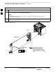
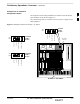
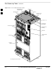
Before applying any power to the BTS frame, follow the procedure in
Table 2-2 while referring to Figure 2-3 and Figure 2-4 for +27 V
systems or to Figure 2-5 and Figure 2-6 for –48 V systems to verify
there are no shorts in the BTS frame DC distribution system.
Table 2-2: DC Power Pre–test (BTS Frame)
Step Action
1 Physically verify that all DC power sources supplying power to the frame are OFF or disabled.
2 On each frame:
Unseat all circuit boards (except CCD and CIO cards) in the C–CCP shelf and LPA shelves, but
leave them in their associated slots.
Set C–CCP shelf breakers to the OFF position by pulling out power distribution breakers (labeled
C–CCP 1, 2, 3 on the +27 V BTS C–CCP power distribution panel and labeled POWER
1,4,5,2,6,7,3,8,9 on the –48 V C–CCP power distribution panel).
Set LPA breakers to the OFF position by pulling out the LPA breakers (8 breakers, labeled 1A–1B
through 4C–4D – located on the C–CCP power distribution panel in the +27 V BTS or on the
power conversion shelf power distribution panel in the –48 V BTS).
3 Verify that the resistance from the power (+ or –) feed terminals with respect to the ground terminal on
the top of the frame measures >
500 Ω (see Figure 2-3).
If reading is < 500 Ω, a short may exist somewhere in the DC distribution path supplied by the
breaker. Isolate the problem before proceeding. A reading > 3 M
Ω could indicate an open (or
missing) bleeder resistor (installed across the filter capacitors behind the breaker panel).
4 Set the C–CCP (POWER) breakers to the ON position by pushing them IN one at a time. Repeat
Step 3 after turning on each breaker.
* IMPORTANT* IMPORTANT
If the ohmmeter stays at 0 Ω after inserting any board/module, a short probably exists in that
board/module. Replace the suspect board/module and repeat the test. If test still fails, isolate the
problem before proceeding.
5 Insert and lock the DC/DC converter modules for the C–CCP shelf and into their associated slots one
at a time. Repeat Step 3 after inserting each module.
A typical response is that the ohmmeter steadily climbs in resistance as capacitors charge, finally
indicating approximately 500
Ω.
! CAUTION
Verify the correct power/converter modules by observing the locking/retracting tabs appear as follows:
–
(in +27 V BTS C–CCP shelf)
–
(in –48 V BTS C–CCP shelf)
STPN4045A
PWR CONV CDMA RCVR
STPN4009
PWR CONV CDMA RCVR
6 Insert and lock all remaining circuit boards and modules into their associated slots in the C–CCP shelf.
Repeat Step 3 after inserting and locking each board or module.
A typical response is that the ohmmeter steadily climbs in resistance as capacitors charge, stopping
at approximately 500
Ω..
. . . continued on next page
2