Chapter 2: Preliminary Operations Table of Contents Mar 2001 Preliminary Operations: Overview . . . . . . . . . . . . . . . . . . . . . . . . . . . . . . . . . . . Introduction . . . . . . . . . . . . . . . . . . . . . . . . . . . . . . . . . . . . . . . . . . . . . . Cell Site Types . . . . . . . . . . . . . . . . . . . . . . . . . . . . . . . . . . . . . . . . . . . . CDF . . . . . . . . . . . . . . . . . . . . . . . . . . . . . . . . . . . . . . . . . . . . . . . . . . . . Site Equipage Verification .
Table of Contents – continued Notes 2 SCt4812T CDMA BTS Optimization/ATP Mar 2001 DRAFT
Preliminary Operations: Overview Introduction This section first verifies proper frame equipage. This includes verifying module placement, jumper, and dual in–line package (DIP) switch settings against the site-specific documentation supplied for each BTS application. Next, pre-power up and initial power-up procedures are presented. Cell Site Types Sites are configured as Omni with a maximum of 4 carriers, 3–sectored with a maximum of 4 carriers, and 6–sectored with a maximum of 2 carriers.
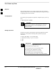
Preliminary Operations: Overview – continued Table 2-1: Initial Installation of Boards/Modules Step 2 1 Action Refer to the site documentation and install all boards and modules into the appropriate shelves as required. Verify they are NOT SEATED at this time. NOTE On 800 MHz systems, the Switch Card has a configuration switch that must match the site configuration (see Figure 2-1).
Preliminary Operations: Overview – continued Setting Frame C–CCP Shelf Configuration Switch The backplane switch settings behind the fan module nearest the breaker panel should be set as shown in Figure 2-2. The switch setting must be verified and set before power is applied to the BTS equipment.
Pre–Power–up Tests Objective 2 This procedure checks for any electrical short circuits and verifies the operation and tolerances of the cellsite and BTS power supply units prior to applying power for the first time. Test Equipment The following test equipment is required to complete the pre–power–up tests: Digital Multimeter (DMM) CAUTION Always wear a conductive, high impedance wrist strap while handling the any circuit card/module to prevent damage by ESD.
Pre–Power–up Tests – continued DC Power Pre-test (BTS Frame) Before applying any power to the BTS frame, follow the procedure in Table 2-2 while referring to Figure 2-3 and Figure 2-4 for +27 V systems or to Figure 2-5 and Figure 2-6 for –48 V systems to verify there are no shorts in the BTS frame DC distribution system. 2 Table 2-2: DC Power Pre–test (BTS Frame) Step Action 1 Physically verify that all DC power sources supplying power to the frame are OFF or disabled.
Pre–Power–up Tests – continued Table 2-2: DC Power Pre–test (BTS Frame) Step 2 7 Action Set the LPA breakers ON by pushing them IN one at a time. Repeat Step 3 after turning on each breaker. A typical response is that the ohmmeter will steadily climb in resistance as capacitors charge, stopping at approximately 500 Ω.. 8 In the –48 V BTS, insert and lock the DC/DC LPA converter modules into their associated slots one at a time. Repeat Step 3 after inserting each module.
Pre–Power–up Tests – continued Figure 2-3: +27 V BTS DC Distribution Pre-test TOP OF FRAME 2C 30 2D 3A 30 3B 3C 30 3D 4A 30 4B 4C 30 4D 1 50 2 50 3 50 4 2B 1 30 5 2A 2 1D 6 30 LIVE TERMINALS 3 1C +27 VDC GND L P A 1B CAUTION LPA BREAKERS 30 LFR/ HSO LIVE TERMINALS 1A 2 TX OUT FW00298 POWER INPUT C–CCP BREAKERS C C C P BREAKER PANEL Breakering: Two LPAs on each trunking backplane breakered together Designed for peak LPA current of 15 amps (30 amp breake
Pre–Power–up Tests – continued Figure 2-4: +27 V SC 4812T BTS Starter Frame Span I/O A RGD (Needed for Expansion only) 2 Site I/O ÂÂÂÂÂÂÂÂÂÂÂÂ ÂÂÂÂÂÂÂÂÂÂÂÂ ÂÂÂÂÂÂÂÂÂÂÂÂ ÂÂÂÂÂÂÂÂÂÂÂÂ ÂÂÂÂÂÂÂÂÂÂÂÂ ÂÂÂÂÂÂÂÂÂÂÂÂ ÂÂÂÂÂÂÂÂÂÂÂÂ Á Span I/O B Exhaust Region RX In (1A – 6A and 1B – 6B) TX Out (1 – 6) Power Input Connection C–CCP Cage ÁÁ Á Expansion I/O Housing Á Á Breakers Front Cosmetic Panel LPA Cage Combiner Section For clarity, doors are not shown.
Pre–Power–up Tests – continued Figure 2-5: –48 V BTS DC Distribution Pre-test TOP OF FRAME LIVE TERMINALS WIRED FOR –48 VDC 2 LIVE TERMINALS HSO/ LFR 3 2 1 3 2 1 1 5 4 6 2 3 GND CAUTION TX OUT P O W E R 1 30 4 40 5 40 2 30 6 40 7 40 3 POWER INPUT L P A 30 8 40 9 40 C–CCP BREAKER 1A 30 1B 1C 30 1D 2A 30 2B 2C 30 2D 3A 30 3B 3C 30 3D 4A 30 4B 4C 30 4D LPA BREAKER Breakering: Two LPAs on each trunking backplane breakered together Designed f
Pre–Power–up Tests – continued Figure 2-6: –48 V SC 4812T BTS Starter Frame Alarms RGD (Needed for Expansion only) 2 ÂÂÂÂÂÂÂÂÂÂ ÂÂÂÂÂÂÂÂÂÂ ÂÂÂÂÂÂÂÂÂÂ ÂÂÂÂÂÂÂÂÂÂ ÂÂÂÂÂÂÂÂÂÂ ÂÂÂÂÂÂÂÂÂÂ ÂÂÂÂÂÂÂÂÂÂ Á ÁÁ Á ÁÁ Á Exhaust Region C–CCP Cage Span I/O A Site I/O Span I/O B RX In (1A – 6A and 1B – 6B) TX Out (1 – 6) Power Input Connection Expansion I/O Housing Breakers Front Cosmetic Panel LPA Cage Combiner Section Power Conversion Shelf Á Breakers For clarity, doors are not shown.
Pre–Power–up Tests – continued DC Power Pre-test (RFDS) Before applying power to the RFDS, follow the steps in Table 2-3, while referring to Figure 2-7, to verify there are no shorts in the RFDS DC distribution system, backplanes, or modules/boards. As of the date of this publication, the RFDS is not used with the –48 V BTS. IMPORTANT * Visual inspection of card placement and equipage for each frame vs.
Initial Power–up Tests Power-up Procedures 2 WARNING Potentially lethal voltage and current levels are routed to the BTS equipment. This test must be performed with a second person present, acting in a safety role. Remove all rings, jewelry, and wrist watches prior to beginning this test. DC Input Power In the tests to follow, power will first be verified at the input to each BTS frame. After power is verified, cards and modules within the frame itself will be powered up and verified one at a time.
Initial Power–up Tests – continued Table 2-4: DC Input Power Cable Guidelines Maximum Cable Length Wire Size 30.38 m (100 ft) 107 mm2 (AWG #4/0) 54.864 m (180 ft) 185 mm2 (350 kcmil) Greater that 54.864 m (180 ft) Not recommended 2 IMPORTANT * If Anderson SB350 style power connectors are used, make sure the connector adapters are securely attached to each of the BTS power feeds and returns. Also, make sure the cables have been properly installed into each connector.
Initial Power–up Tests – continued Initial Power-up (RFDS) The procedure in Table 2-6 must be performed on the RFDS after input power from the common power supply has been verified. Perform the following steps to apply initial power to the cards/modules within the frame itself, verifying that each is operating within specification. 2 IMPORTANT * Visual inspection of card placement and equipage for each frame vs.
Initial Power–up Tests – continued Table 2-7: Initial Power–up (BTS) Step 5 Action Seat the first equipped LPA module pair into the assigned slot in the upper LPA shelf including LPA fan. In +27 V systems, observe that the LPA internal fan comes on line. 6 Repeat step 5 for all remaining LPAs. 7 Set the LPA breakers to the ON position (per configuration) by pushing them IN one at a time.
Initial Power–up Tests – continued Notes 2 2-16 SCt4812T CDMA BTS Optimization/ATP Mar 2001 DRAFT
Chapter 3: Optimization/Calibration Table of Contents 3 Mar 2001 Optimization/Calibration – Introduction . . . . . . . . . . . . . . . . . . . . . . . . . . . . . . Introduction . . . . . . . . . . . . . . . . . . . . . . . . . . . . . . . . . . . . . . . . . . . . . . Optimization Process . . . . . . . . . . . . . . . . . . . . . . . . . . . . . . . . . . . . . . . Cell Site Types . . . . . . . . . . . . . . . . . . . . . . . . . . . . . . . . . . . . . . . . . . . . Cell–Site Data File . . . . . . . .
Table of Contents 3 – continued Null Modem Cable . . . . . . . . . . . . . . . . . . . . . . . . . . . . . . . . . . . . . . . . CSM Frequency Verification . . . . . . . . . . . . . . . . . . . . . . . . . . . . . . . . . Test Equipment Setup: GPS & LFR/HSO Verification . . . . . . . . . . . . . GPS Initialization/Verification . . . . . . . . . . . . . . . . . . . . . . . . . . . . . . . . LFR Initialization/Verification . . . . . . . . . . . . . . . . . . . . . . . . . . . . . . . .
Table of Contents Mar 2001 – continued Set Antenna Map Data . . . . . . . . . . . . . . . . . . . . . . . . . . . . . . . . . . . . . . Set RFDS Configuration Data . . . . . . . . . . . . . . . . . . . . . . . . . . . . . . . . RFDS Calibration . . . . . . . . . . . . . . . . . . . . . . . . . . . . . . . . . . . . . . . . . Program TSU NAM . . . . . . . . . . . . . . . . . . . . . . . . . . . . . . . . . . . . . . . . 3-80 3-81 3-82 3-83 BTS Redundancy/Alarm Testing . . . . . . . . . . . . . . . . . .
Table of Contents – continued Notes 3 SCt4812T CDMA BTS Optimization/ATP Mar 2001 DRAFT
Optimization/Calibration – Introduction Introduction This section describes procedures for isolating the BTS from the span lines, preparing and using the LMF, downloading system operating software, CSM reference verification/optimization, set up and calibration of the supported test equipment, transmit/receive path verification, using the RFDS, and verifying the customer defined alarms and relay contacts are functioning properly.
Optimization/Calibration – Introduction – continued 10. Select all of the BBXs and all of the MCCs, and use the full optimization function. The full optimization function performs TX calibration, BLO download, TX audit, all TX tests, and all RX tests for all selected devices. 11. If the TX calibration fails, repeat the full optimization for any failed paths. 12. If the TX calibration fails again, correct the problem that caused the failure and repeat the full optimization for the failed path. 3 13.
Optimization/Calibration – Introduction – continued Effective Rated Power (ERP) table for all TX channels to antennas respectively. Motorola System Engineering specifies the ERP of a transmit antenna based on site geography, antenna placement, and government regulations. Working from this ERP requirement, the antenna gain, (dependent on the units of measurement specified) and antenna feed line loss can be combined to determine the required power at the top of the BTS frame.
Isolate Span Lines/Connect LMF Isolate BTS from T1/E1 Spans IMPORTANT * 3 At active sites, the OMC/CBSC must disable the BTS and place it out of service (OOS). DO NOT remove the 50–pin TELCO cable connected to the BTS frame site I/O board J1 connector until the OMC/CBSC has disabled the BTS! Each frame is equipped with one Site I/O and two Span I/O boards. The Span I/O J1 connector provides connection of 25 pairs of wire. A GLI2 card can support up to six spans.
Isolate Span Lines/Connect LMF – continued Figure 3-1: Span I/O Board T1 Span Isolation 50–PIN TELCO CONNECTORS REMOVED SPAN A CONNECTOR (TELCO) INTERFACE TO SPAN LINES 3 SPAN B CONNECTOR (TELCO) INTERFACE TO SPAN LINES RS–232 9–PIN SUB D CONNECTOR SERIAL PORT FOR EXTERNAL DIAL UP MODEM CONNECTION (IF USED) TOP of Frame (Site I/O and Span I/O boards) FW00299 LMF to BTS Connection The LMF is connected to the LAN A or B connector located on the left side of the frame’s lower air intake grill, behind the
Isolate Span Lines/Connect LMF – continued Figure 3-2: LMF Connection Detail NOTE: Open LAN CABLE ACCESS door. Pull apart Velcro tape and gain access to the LAN A or LAN B LMF BNC connector.
Preparing the LMF Overview Software and files for installation and updating of the LMF are provided on CD ROM disks. The following installation items must be available: LMF Program on CD ROM LMF Binaries on CD ROM CDF for each supported BTS (on diskette or available from the 3 CBSC) CBSC File for each supported BTS (on diskette or available from the CBSC) The following section provides information and instructions for installing and updating the LMF software and files.
Preparing the LMF – continued Table 3-3: LMF Operating System Installation Step 5 Action Follow the instructions displayed on the Setup screen.
Preparing the LMF – continued IMPORTANT * When copying CDF files, comply with the following to prevent BTS login problems with the LMF: – The numbers used in the bts–#.cdf and cbsc–#.cdf filenames must correspond to the locally assigned numbers for each BTS and its controlling CBSC. – The generic cbsc–1.cdf file supplied with the LMF work with locally numbered BTS CDF files. Using this file does not provide a valid optimization unless the generic file is edited to replace default parameters (e.g.
Preparing the LMF – continued Table 3-4: Copying CBSC CDF Files to the LMF Step 3 Action 8 Repeat steps 5 through 7 for each bts–# that must be supported by the LMF. 9 When all required files have been copied to the diskette, type eject and press the key. 10 Remove the diskette from the CBSC. AT THE LMF: 11 Start the Windows operating system. 12 Insert the diskette into the LMF. 13 Using Windows Explorer (or equivalent program), create a corresponding bts–# folder in the wlmf\cdma
Preparing the LMF – continued Table 3-5: Creating a Named Hyperlink Connection for MMI Connection Step Action 1 From the Windows Start menu, select: Programs>Accessories 2 Perform one of the following: For Win NT, select Hyperterminal and then click on HyperTerminal For Win 98, select Communications, double click the Hyperterminal folder, and then double click on the Hyperterm.exe icon in the window that opens.
Preparing the LMF – continued Table 3-5: Creating a Named Hyperlink Connection for MMI Connection Step 10 Action Perform one of the following: If the Hyperterminal folder window is still open (Win 98) proceed to step 12 From the Windows Start menu, select Programs > Accessories 11 3 Perform one of the following: For Win NT, select Hyperterminal and release any pressed mouse buttons. For Win 98, select Communications and double click the Hyperterminal folder.
Preparing the LMF – continued Folder Structure Overview The LMF uses a wlmf folder that contains all of the essential data for installing and maintaining the BTS. The list that follows outlines the folder structure for the LMF. Except for the bts–nnn folders, these folders are created as part of the the LMF installation. Refer to the CDMA LMF Operator’s Guide for a complete description of the folder structure.
Preparing the LMF – continued Pinging the Processors For proper operation, the integrity of the Ethernet LAN A and B links must be be verified. Figure 3-4 represents a typical BTS Ethernet configuration. The drawing depicts one (of two identical) links, A and B. Ping is a program that routes request packets to the LAN network modules to obtain a response from the specified “targeted” BTS.
Preparing the LMF – continued Table 3-6: Pinging the Processors Step Action 1 If you have not already done so, connect the LMF to the BTS (see Table 3-2 on page 3-5). 2 From the Windows desktop, click the Start button and select Run. 3 In the Open box, type ping and the (for example, ping 128.0.0.2). NOTE 128.0.0.2 is the default IP address for MGLI–1 in field BTS units. 128.0.0.1 is the default IP address for MGLI–2. 4 Click on the OK button.
Preparing the LMF – continued Figure 3-5: +27 V SC 4812T Starter Frame I/O Plate ALARM B SPAN I/O B SITE I/O TOP VIEW 3-16 SCt4812T CDMA BTS Optimization/ATP 5 3 6 2B GND RX 3A 3B 4A 4B 5A 5B 6A 6B CAUTION EXP I/O FRONT 2 LFR/ HSO LIVE TERMINALS SPAN I/O A 2A 1B 4 +27 VDC RGD 3 RGPS 1A 1 LIVE TERMINALS ÄÄÄÄÄÄÄÄÄÄÄÄÄÄÄÄÄÄÄ ÄÄÄÄÄÄÄÄÄÄÄÄÄÄÄÄÄÄÄ ÄÄÄÄÄÄÄÄÄÄÄÄÄÄÄÄÄÄÄ ÄÄÄÄÄÄÄÄÄÄÄÄÄÄÄÄÄÄÄ ÄÄÄÄÄÄÄÄÄÄÄÄÄÄÄÄÄÄÄ ÄÄÄÄÄÄÄÄÄÄÄÄÄÄÄÄÄÄÄ ÄÄÄÄÄÄÄÄÄÄÄÄÄÄÄÄÄÄÄ ÄÄÄÄÄÄÄÄÄÄÄÄÄÄÄÄÄÄÄ ÄÄÄÄÄÄÄÄÄÄ
Preparing the LMF – continued Figure 3-6: –48 V SC 4812T Starter Frame I/O Plate REAR SPAN I/O A SITE I/O 1B 2A 2B 3A 3B HSO/ LFR GND 4 2 5 3 6 3 SPAN I/O B FRONT 4A 4B 5A 5B 6A 6B RX LIVE TERMINALS RGD RGPS 1A 1 1 2 3 –48 VDC SPAN I/O A ALARM A LIVE TERMINALS SITE I/O ÄÄÄÄÄÄÄÄÄÄÄÄÄÄÄÄÄÄÄ ÄÄÄÄÄÄÄÄÄÄÄÄÄÄÄÄÄÄÄ ÄÄÄÄÄÄÄÄÄÄÄÄÄÄÄÄÄÄÄ ÄÄÄÄÄÄÄÄÄÄÄÄÄÄÄÄÄÄÄ ÄÄÄÄÄÄÄÄÄÄÄÄÄÄÄÄÄÄÄ ÄÄÄÄÄÄÄÄÄÄÄÄÄÄÄÄÄÄÄ ÄÄÄÄÄÄÄÄÄÄÄÄÄÄÄÄÄÄÄ ÄÄÄÄÄÄÄÄÄÄÄÄÄÄÄÄÄÄÄ ÄÄÄÄÄÄÄÄÄÄÄÄÄÄÄÄÄÄÄ ÄÄÄÄÄÄÄÄÄÄÄÄÄÄÄÄÄÄÄ ÄÄÄÄÄÄ
Using CDMA LMF Basic LMF Operation The CDMA LMF allows the user to work in the two following operating environments, which are accessed using the specified desktop icon: Graphical User Interface (GUI) using the WinLMF icon Command Line Interface (CLI) using the WinLMF CLI icon The GUI is the primary optimization and acceptance testing operating environment.
Using CDMA LMF – continued Command Line Interface Overview The LMF also provides Command Line Interface (CLI) capability. Activate the CLI by clicking on a shortcut icon on the desktop. The CLI can not be launched from the GUI, only from the desktop icon. Both the GUI and the CLI use a program known as the handler. Only one handler can be running at one time Due to architectural limitations, the GUI must be started before the CLI if you want the GUI and CLI to use the same handler.
Using CDMA LMF – continued Logging into a BTS IMPORTANT * 3 Be sure that the correct bts–#.cdf and cbsc–#.cdf file is used for the BTS. These should be the CDF files that are provided for the BTS by the CBSC. Failure to use the correct CDF files can result in invalid optimization. Failure to use the correct CDF files to log into a live (traffic carrying) site can shut down the site. Logging into a BTS establishes a communications link between the BTS and the CDMA LMF.
Using CDMA LMF – continued Table 3-7: BTS GUI Login Procedure Step Action 3 If no base stations are displayed in the Available Base Stations pick list, double click on the CDMA icon. 4 Click on the desired BTS number. 5 Click on the Network Login tab (if not already in the forefront). 6 Enter the correct IP address (normally 128.0.0.2 for a field BTS) if not correctly displayed in the IP Address box. NOTE 128.0.0.2 is the default IP address for MGLI–1 in field BTS units. 128.0.0.
Using CDMA LMF – continued BTS Login from the CLI Environment Follow the procedure in Table 3-8 to log into a BTS when using the CLI environment. IMPORTANT * 3 The GUI and CLI environments use the same connection to a BTS. If a GUI and the CLI session are running for the same BTS at the same time, logging out of the BTS in either environment will log out of it for both. When either a login or logout is performed in the CLI window, there is no GUI indication that logout has occurred.
Using CDMA LMF – continued Table 3-9: BTS GUI Logout Procedure Step Action 1 Click on Select on the BTS tab menu bar. 2 Click the Logout item in the pull–down menu (a Confirm Logout pop–up message appears). 3 Click on Yes or press the key to confirm logout. You are returned to the Login tab. 3 NOTE If a logout was previously performed on the BTS from a CLI window running at the same time as the GUI, a Logout Error pop–up message appears stating the system should not log out of the BTS.
Using CDMA LMF – continued Logging Out of a BTS from the CLI Environment Follow the procedure in Table 3-9 to logout of a BTS when using the CLI environment. Table 3-10: BTS CLI Logout Procedure Step Action * IMPORTANT 3 If the BTS is also logged into from a GUI running at the same time and further work must be done with it in the GUI, proceed to step 2. 1 Logout of a BTS by entering the following command: logout bts– A response similar to the following is displayed: LMF> 12:22:58.
Using CDMA LMF – continued Establishing an MMI Communication Session For those procedures that require MMI communications between the LMF and BTS FRUs, follow the procedure in Table 3-11 to initiate the communication session. Table 3-11: Establishing MMI Communications Step Action 3 1 Connect the LMF computer to the equipment as detailed in the applicable procedure that requires the MMI communication session.
Download the BTS Download the BTS – Overview Before a BTS can operate, each equipped device must contain device initialization (ROM) code. ROM code is loaded in all devices during manufacture or factory repair. Device application (RAM) code and data must be downloaded to each equipped device by the user before the BTS can be made fully functional for the site where it is installed.
Download the BTS – continued Download Code to Devices Code can be downloaded to a device that is in any state. After the download starts, the device being downloaded changes to OOS_ROM (blue). If the download is completed successfully, the device changes to OOS_RAM with code loaded (yellow). Prior to downloading a device, a code file must exist. The code file is selected automatically if the code file is in the /lmf/cdma/n.n.n.n/code folder (where n.n.n.
Download the BTS – continued WARNING R9 RAM code must NOT be downloaded to a device that has R8 ROM code and R8 RAM code must NOT be downloaded to a device that has R9 ROM code. All devices in a BTS must have the same R–level ROM and RAM code before the optimization and ATP procedures can be performed. If a newly installed R8 BTS is to be upgraded to R9, the optimization and ATPs should be accomplished with the R8 code. Then the site should be upgraded to R9 by the CBSC.
Download the BTS – continued Download Code and Data to Non–MGLI2 Devices Non–MGLI2 devices can be downloaded individually or all equipped devices can be downloaded with one action. Follow the procedure in Table 3-13 to download code and data to the non–MGLI2 devices. NOTE When downloading multiple devices, the download may fail for some of the devices (a time out occurs). These devices can be downloaded separately after completing the multiple download.
Download the BTS – continued Follow the procedure in Table 3-14 to select a CSM Clock Source. Table 3-14: Select CSM Clock Source Step 3 Action 1 Select the applicable CSM(s). 2 Click on the Device menu. 3 Click on the Clock Source menu item. 4 Click on the Select menu item. A clock source selection window is displayed. Select the applicable clock source in the Clock Reference Source pick lists. Uncheck the related check box if you do not want the displayed pick list item to be used.
Download the BTS – continued Follow the procedure in Table 3-15 to enable the CSMs. Table 3-15: Enable CSMs Step Action 1 Verify the CSM(s) have been downloaded with code (Yellow, OOS–RAM) and data. 2 Click on the target CSM. From the Device pull down, select Enable. 3 NOTE If equipped with two CSMs, enable CSM–2 first and then CSM–1. A status report confirms change in the device(s) status. Click OK to close the status window. NOTE FAIL may be shown in the status table for enable action.
Download the BTS – continued Enable MCCs This procedure configures the MCC and sets the “tx fine adjust” parameter. The “tx fine adjust” parameter is not a transmit gain setting, but a timing adjustment that compensates for the processing delay in the BTS (approximately 3 ms). Follow the procedure in Table 3-16 to enable the MCCs. IMPORTANT 3 * The MGLI2, and primary CSM must be downloaded and enabled (IN–SERVICE ACTIVE), before downloading and enabling the MCC.
CSM System Time/GPS and LFR/HSO Verification CSM & LFR Background The primary function of the Clock Synchronization Manager (CSM) boards (slots 1 and 2) is to maintain CDMA system time. The CSM in slot 1 is the primary timing source while slot 2 provides redundancy. The CSM2 card (CSM second generation) is required when using the remote GPS receiver (R–GPS). R–GPS uses a GPS receiver in the antenna head that has a digital output to the CSM2 card.
CSM System Time/GPS and LFR/HSO Verification – continued Low Frequency Receiver/ High Stability Oscillator The CSM handles the overall configuration and status monitoring functions of the LFR/HSO. In the event of GPS failure, the LFR/HSO is capable of maintaining synchronization initially established by the GPS reference signal. The LFR requires an active external antenna to receive LORAN RF signals.
CSM System Time/GPS and LFR/HSO Verification – continued Null Modem Cable A null modem cable is required. It is connected between the LMF COM1 port and the RS232–GPIB Interface box. Figure 3-8 shows the wiring detail for the null modem cable.
CSM System Time/GPS and LFR/HSO Verification – continued Table 3-18: Test Equipment Setup (GPS & LFR/HSO Verification) Step Action 3 Reinstall CSM–2. 4 Start an MMI communication session with CSM–1 by using the Windows desktop shortcut icon (see Table 3-5) NOTE The LMF program must not be running when a Hyperterminal session is started if COM1 is being used for the MMI session. 3 When the terminal screen appears, press the key until the CSM> prompt appears.
CSM System Time/GPS and LFR/HSO Verification – continued GPS Initialization/Verification Follow the procedure in Table 3-19 to initialize and verify proper GPS receiver operation. Prerequisites Ensure the following prerequisites have been met before proceeding: The LMF is not logged into the BTS. The COM1 port is connected to the MMI port of the primary CSM via a null modem board (see Figure 3-9). The primary CSM and HSO (if equipped) have been warmed up for at least 15 minutes.
CSM System Time/GPS and LFR/HSO Verification – continued Table 3-19: GPS Initialization/Verification Step Action 3 Verify the following GPS information (underlined text above): – GPS information is usually the 0 reference source. – At least one Primary source must indicate “Status = good” and “Valid = yes” to bring site up. 4 Enter the following command at the CSM> prompt to verify that the GPS receiver is in tracking mode.
CSM System Time/GPS and LFR/HSO Verification – continued Table 3-19: GPS Initialization/Verification Step 6 Action If steps 1 through 5 pass, the GPS is good. * IMPORTANT If any of the above mentioned areas fail, verify that: – If Initial position accuracy is “estimated” (typical), at least 4 satellites must be tracked and visible (1 satellite must be tracked and visible if actual lat, log, and height data for this site has been entered into CDF file).
CSM System Time/GPS and LFR/HSO Verification – continued LFR Initialization/Verification The LORAN–C LFR is a full size card that resides in the C–CCP Shelf. The LFR is a completely self-contained unit that interfaces with the CSM via a serial communications link. The CSM handles the overall configuration and status monitoring functions of the LFR.
CSM System Time/GPS and LFR/HSO Verification – continued Table 3-20: LFR Initialization/Verification Step Action 1 At the CSM> prompt, enter lstatus to verify that the LFR is in tracking mode.
CSM System Time/GPS and LFR/HSO Verification – continued Table 3-20: LFR Initialization/Verification Step Action Note 2 Verify the following LFR information (highlighted above in boldface type): – Locate the “dot” that indicates the current phase locked station assignment (assigned by MM). – Verify that the station call letters are as specified in site documentation as well as M X Y Z assignment. – Verify the signal to noise (S/N) ratio of the phase locked station is greater than 8.
CSM System Time/GPS and LFR/HSO Verification – continued HSO Initialization/Verification The HSO module is a full–size card that resides in the C–CCP Shelf. This completely self contained high stability 10 MHz oscillator interfaces with the CSM via a serial communications link. The CSM handles the overall configuration and status monitoring functions of the HSO.
Test Equipment Set–up Connecting Test Equipment to the BTS All test equipment is controlled by the LMF via an IEEE–488/GPIB bus. The LMF requires each piece of test equipment to have a factory set GPIB address. If there is a communications problem between the LMF and any piece of test equipment, verify that the GPIB addresses have been set correctly (normally 13 for a power meter and 18 for a CDMA analyzer).
Test Equipment Set–up – continued Test Equipment Reference Chart Table 3-22 depicts the current test equipment available meeting Motorola standards. To identify the connection ports, locate the test equipment presently being used in the TEST SETS columns, and read down the column. Where a ball appears in the column, connect one end of the test cable to that port. Follow the horizontal line to locate the end connection(s), reading up the column to identify the appropriate equipment/BTS port.
Test Equipment Set–up – continued Equipment Warm-up IMPORTANT * 3 Warm-up BTS equipment for a minimum of 60 minutes prior to performing the BTS optimization procedure. This assures BTS site stability and contributes to optimization accuracy. (Time spent running initial power-up, hardware/firmware audit, and BTS download counts as warm-up time.) Calibrating Cables Figure 3-10 shows the cable calibration setup for various supported test sets.
Test Equipment Set–up – continued Figure 3-10: Cable Calibration Test Setup SUPPORTED TEST SETS CALIBRATION SET UP Motorola CyberTest A. SHORT CABLE CAL ÏÏÏÏ ÏÏÏÏÌ ANT IN SHORT CABLE TEST SET 3 RF GEN OUT Note: The Directional Coupler is not used with the Cybertest Test Set. The TX cable is connected directly to the Cybertest Test Set. B. RX TEST SETUP A 10dB attenuator must be used with the short test cable for cable calibration with the CyberTest Test Set.
Test Equipment Set–up – continued Setup for TX Calibration Figure 3-11 and Figure 3-12 show the test set connections for TX calibration. Figure 3-11: TX Calibration Test Setup (CyberTest, HP 8935, and Advantest) TEST SETS 3 TRANSMIT (TX) SET UP Motorola CyberTest POWER SENSOR 100–WATT (MIN) NON–RADIATING RF LOAD ÏÏÏ ÏÏÏÌ FRONT PANEL POWER METER (OPTIONAL)* OUT RF IN/OUT 2O DB PAD (FOR 1.7/1.9 GHZ) NOTE: THE DIRECTIONAL COUPLER IS NOT USED WITH THE CYBERTEST TEST SET.
Test Equipment Set–up – continued Figure 3-12: TX Calibration Test Setup HP 8921A W/PCS for 1.7/1.9 GHz TEST SETS TRANSMIT (TX) SET UP Hewlett–Packard Model HP 8921A W/PCS Interface 100–WATT (MIN) NON–RADIATING RF LOAD POWER SENSOR 30 DB DIRECTIONAL COUPLER WITH UNUSED PORT TERMINATED POWER METER 3 TX TEST CABLE 2O DB PAD Note: The HP 8921A cannot be used for TX calibration. A power meter must be used.
Test Equipment Set–up – continued Setup for Optimization/ATP Figure 3-13 and Figure 3-14 show the test set connections for optimization/ATP tests. Figure 3-13: Optimization/ATP Test Setup Calibration (CyberTest, HP 8935 and Advantest) TEST SETS 3 Optimization/ATP SET UP Motorola CyberTest SYNC MONITOR EVEN SEC TICK PULSE REFERENCE FROM CSM BOARD FREQ MONITOR 19.
Test Equipment Set–up – continued Figure 3-14: Optimization/ATP Test Setup HP 8921A TEST SETS Optimization/ATP SET UP Hewlett–Packard Model HP 8921A W/PCS Interface (for 1700 and 1900 MHz) SYNC MONITOR EVEN SEC TICK PULSE REFERENCE FROM CSM BOARD FREQ MONITOR 19.6608 MHZ CLOCK REFERENCE FROM CSM BOARD NOTE: IF BTS RX/TX SIGNALS ARE DUPLEXED (4800E): BOTH THE TX AND RX TEST CABLES CONNECT TO THE DUPLEXED ANTENNA GROUP.
Test Equipment Set–up – continued Figure 3-15: Typical TX ATP Setup with Directional Coupler (shown with and without RFDS) TX ANTENNA DIRECTIONAL COUPLERS COBRA RFDS Detail RX (RFM TX) TX RF FROM BTS FRAME 3 TX (RFM RX) 2 1 RFDS RX (RFM TX) COUPLER OUTPUTS TO RFDS FWD(BTS) ASU2 (SHADED) CONNECTORS 3 RF FEED LINE TO DIRECTIONAL COUPLER REMOVED Connect TX test cable between the directional coupler input port and the appropriate TX antenna directional coupler connector.
Test Equipment Set–up – continued Figure 3-16: Typical RX ATP Setup with Directional Coupler (shown with or without RFDS) COBRA RFDS Detail RX ANTENNA DIRECTIONAL COUPLERS RX RF FROM BTS FRAME 2 3 4 5 6 RX (RFM TX) 1 TX (RFM RX) RFDS TX (RFM RX) COUPLER OUTPUTS TO RFDS FWD(BTS) ASU1 (SHADED) CONNECTORS 3 RF FEED LINE TO TX ANTENNA REMOVED Connect RX test cable between the test set and the appropriate RX antenna directional coupler.
Test Set Calibration Test Set Calibration Background Proper test equipment calibration ensures that the test equipment and associated test cables do not introduce measurement errors, and that measurements are correct. NOTE 3 If the test set being used to interface with the BTS has been calibrated and maintained as a set, this procedure does not need to be performed. (Test Set includes LMF terminal, communications test set, additional test equipment, associated test cables, and adapters.
Test Set Calibration – continued Selecting Test Equipment Use LMF Options from the Options menu list to select test equipment automatically (using the autodetect feature) or manually. A Serial Connection and a Network Connection tab are provided for test equipment selection. The Serial Connection tab is used when the test equipment items are connected directly to the LMF computer via a GPIB box (normal setup).
Test Set Calibration – continued Automatically Selecting Test Equipment in a Serial Connection Tab When using the auto-detection feature to select test equipment, the LMF examines which test equipment items are actually communicating with the LMF. Follow the procedure in Table 3-24 to use the auto-detect feature. Table 3-24: Selecting Test Equipment Using Auto-Detect 3 Step Action 1 From the Options menu, select LMF Options. The LMF Options window appears.
Test Set Calibration – continued Calibrating Test Equipment The calibrate test equipment function zeros the power measurement level of the test equipment item that is to be used for TX calibration and audit. If both a power meter and an analyzer are connected, only the power meter is zeroed. Use the Calibrate Test Equipment menu item from the Util menu to calibrate test equipment. The test equipment must be selected before calibration can begin.
Test Set Calibration – continued The short cable plus the TX cable configuration loss is measured – The TX cable configuration normally consists of two coax cables with type-N connectors and a directional coupler, a load, and an additional attenuator (if required by the specified BTS). The total loss of the path loss of the TX cable configuration must be as required for the BTS (normally 30 or 50 dB).
Test Set Calibration – continued Calibrating TX Cables Using a Signal Generator and Spectrum Analyzer Follow the procedure in Table 3-27 to calibrate the TX cables using a signal generator and spectrum analyzer. Refer to Figure 3-17 for a diagram of the signal generator and spectrum analyzer. Table 3-27: Calibrating TX Cables Using Signal Generator and Spectrum Analyzer Step Action 3 1 Connect a short test cable between the spectrum analyzer and the signal generator.
Test Set Calibration – continued Figure 3-17: Calibrating Test Equipment Setup for TX BLO and TX ATP Tests (using Signal Generator and Spectrum Analyzer) Signal Generator Spectrum Analyzer SHORT TEST CABLE 3 40W NON–RADIATING RF LOAD THIS WILL BE THE CONNECTION TO THE TX PORTS DURING TX BAY LEVEL OFFSET TEST AND TX ATP TESTS.
Test Set Calibration – continued Table 3-28: Calibrating RX Cables Using a Signal Generator and Spectrum Analyzer Step 5 Action Calibration factor = A – B Example: Cal = –12 dBm – (–14 dBm) = 2 dBm NOTE The short test cable is used for test equipment setup calibration only. It is not be part of the final test setup. After calibration is completed, do not re-arrange any cables. Use the equipment setup, as is, to ensure test procedures use the correct calibration factor.
Test Set Calibration – continued Setting Cable Loss Values Cable loss values for the TX and RX test cable configurations are normally set by accomplishing cable calibration using the applicable test equipment. The resulting values are stored in the cable loss files. The cable loss values can also be set/changed manually. Follow the procedure in Table 3-29 to set cable loss values. Prerequisites Logged into the BTS 3 Table 3-29: Setting Cable Loss Values Step Action 1 Click on the Util menu.
Test Set Calibration – continued Setting TX Coupler Loss Value If an in–service TX coupler is installed, the coupler loss (e.g., 30 dB) must be manually entered so it will be included in the LMF TX calibration and audit calculations. Follow the procedure in Table 3-30 to set TX coupler loss values. Prerequisites Logged into the BTS. 3 Table 3-30: Setting TX Coupler Loss Value Step Action 1 Click on the Util menu. 2 Select Edit>TX Coupler Loss. A data entry pop–up window appears.
Bay Level Offset Calibration Introduction to Bay Level Offset Calibration Calibration compensates for normal equipment variations within the BTS and assures maximum measurement accuracy. RF Path Bay Level Offset Calibration 3 Calibration identifies the accumulated gain in every transmit path (BBX slot) at the BTS site and stores that value in a BLO database calibration table in the LMF. The BLOs are subsequently downloaded to each BBX.
Bay Level Offset Calibration – continued – TX filter / TX filter combiner – TX thru-port cable to the top of frame TX Path Calibration The TX Path Calibration assures correct site installation, cabling, and the first order functionality of all installed equipment. The proper function of each RF path is verified during calibration. The external test equipment is used to validate/calibrate the TX paths of the BTS.
Bay Level Offset Calibration – continued BLO Calibration Data File During the calibration process, the LMF creates a bts–n.cal calibration (BLO) offset data file in the bts–n folder. After calibration has been completed, this offset data must be downloaded to the BBXs using the Download BLO function. An explanation of the file is shown below. NOTE 3 Due to the size of the file, Motorola recommends that you print out a hard copy of a bts.cal file and refer to it for the following descriptions.
Bay Level Offset Calibration – continued – The second breakdown of the array is per sector. Configurations supported are Omni, 3–sector or 6–sector. Table 3-32: BTS.
Bay Level Offset Calibration – continued The 20 calibration entries for each sector/branch combination must be stored in order of increasing frequency. If less than 10 points (frequencies) are calibrated, the largest frequency that is calibrated is repeated to fill out the 10 points. Example: C[1]=384, odd cal entry = 1 ‘‘calibration point” C[2]=19102, even cal entry C[3]=777, C[4]=19086, . .
Bay Level Offset Calibration – continued TX Path Calibration The assigned channel frequency and power level (as measured at the top of the frame) for transmit calibration are derived from the site CDF files. For each BBX, the channel frequency is specified in the ChannelList CDF file parameter and the power is specified in the SIFPilotPwr CDF file parameter for the sector associated with the BBX (located under the ParentSECTOR field of the ParentCARRIER CDF file parameter). 3 NOTE If both the BTS–x.
Bay Level Offset Calibration – continued Connect the test equipment as shown in Figure 3-11 and Figure 3-12 and follow the procedure in Table 3-34 to perform the TX calibration test. WARNING Before installing any test equipment directly to any TX OUT connector, first verify there are no CDMA BBX channels keyed. Failure to do so can result in serious personal injury and/or equipment damage. 3 IMPORTANT * Verify all BBX boards removed and repositioned have been returned to their assigned shelves/slots.
Bay Level Offset Calibration – continued Download BLO Procedure After a successful TX path calibration, download the bay level offset (BLO) calibration file data to the BBXs. BLO data is extracted from the CAL file for the Base Transceiver Subsystem (BTS) and downloaded to the selected BBX devices. NOTE If a successful All Cal/Audit was completed, this procedure does not need to be performed, as BLO is downloaded as part of the All Cal/Audit.
Bay Level Offset Calibration – continued TX Path Audit Perform the calibration audit of the TX paths of all equipped BBX slots, per the procedure in Table 3-36 WARNING Before installing any test equipment directly to any TX OUT connector, first verify there are no CDMA BBX channels keyed. Failure to do so can result in serious personal injury and/or equipment damage.
Bay Level Offset Calibration – continued Table 3-36: BTS TX Path Audit Step Action 1 Select the BBX(s) to be audited. 2 From the Tests menu, select TX Audit. 3 4 Select the appropriate carrier(s) displayed in the Channels/Carrier pick list. Press and hold the or key to select multiple items. Type the appropriate channel number in the Carrier n Channels box. 5 Click on OK. 6 Follow the cable connection directions as they are displayed.
Bay Level Offset Calibration – continued Prerequisites Before running this test, ensure that the following have been done: 3 CSM–1, GLI2s, BBXs have correct code and data loads. Primary CSM and MGLI2 are INS. All BBXs are OOS_RAM. Test equipment and test cables are calibrated and connected for TX BLO calibration. LMF is logged into the BTS. Follow the procedure in Table 3-37 to perform the All Cal/Audit test.
Bay Level Offset Calibration – continued Create CAL File The Create Cal File function gets the BLO data from BBXs and creates/updates the CAL file for the BTS. If a CAL file does not exist, a new one is created. If a CAL file already exists, it is updated. After a BTS has been fully optimized, a copy of the CAL file must exist so it can be transferred to the CBSC. If TX calibration has been successfully performed for all BBXs and BLO data has been downloaded, a CAL file exists.
RFDS Setup and Calibration RFDS Description NOTE The RFDS is not available for the –48 V BTS at the time of this publication. 3 The optional RFDS performs RF tests of the site from the CBSC or from an LMF. The RFDS consists of the following elements: Antenna Select Unit (ASU) FWT Interface Card (FWTIC) Subscriber Unit Assembly (SUA) For complete information regarding the RFDS, refer to the CDMA RFDS Hardware Installation manual and CDMA RFDS User’s Guide.
RFDS Setup and Calibration – continued RFDS Parameter Settings The bts-#.cdf file includes RFDS parameter settings that must match the installed RFDS equipment. The paragraphs below describe the editable parameters and their defaults. Table 3-39 explains how to edit the parameter settings. RfdsEquip – valid inputs are 0 through 2.
RFDS Setup and Calibration – continued Table 3-39: RFDS Parameter Settings Step Action * IMPORTANT Log out of the BTS prior to performing this procedure. 1 3 Using a text editor, verify the following fields are set correctly in the bts–#.cdf file (1 = GLI based RFDS; 2 = Cobra RFDS). EXAMPLE: RfdsEquip = 2 TsuEquip = 1 MC1Equip = 0 MC2Equip = 0 MC3Equip = 0 MC4Equip = 0 Asu1Equip = 1 Asu2Equip = 0 (1 if system is non-duplexed) TestOrigDN = ’123456789’’ NOTE The above is an example of the bts-#.
RFDS Setup and Calibration – continued RFDS TSU NAM Programming The RFDS TSU NAM must be programmed with the appropriate system parameters and phone number during hardware installation. The TSU phone and TSU MSI must be recorded for each BTS used for OMC–R RFDS software configuration. The TSU NAM should be configured the same way that any local mobile subscriber would use. NOTE The user will only need to program the NAM for the initial install of the RFDS.
RFDS Setup and Calibration – continued Valid NAM Ranges Table 3-41 provides the valid NAM field ranges. If any of the fields are missing or out of range, the RFDS errors out.
RFDS Setup and Calibration – continued Set Antenna Map Data The antenna map data is only used for RFDS tests and is required if an RFDS is installed. Antenna map data does not have to be entered if an RFDS is not installed. The antenna map data must be entered manually. Perform the procedure in Table 3-42 to set the Antenna Map Data. Prerequisite Logged into the BTS 3 Table 3-42: Set Antenna Map Data Step Action 1 Click on the Util menu. 2 Select Edit>Antenna Map>TX or RX.
RFDS Setup and Calibration – continued Set RFDS Configuration Data If an RFDS is installed, the RFDS configuration data must be manually entered. Perform the procedure in Table 3-43 to set the RFDS Configuration Data. Prerequisite Logged into the BTS. 3 IMPORTANT * The entered antenna# index numbers must correspond to the antenna# index numbers used in the antenna maps. Table 3-43: Set RFDS Configuration Data Step Action 1 Click on the Util menu. 2 Select Edit>RFDS Configuration>TX or RX.
RFDS Setup and Calibration – continued RFDS Calibration The RFDS TX and RX antenna paths must be calibrated to ensure peak performance. The RFDS calibration option calibrates the RFDS TX and RX paths. For a TX antenna path calibration, the BTS XCVR is keyed at a pre–determined power level and the BTS power output level is measured by the RFDS. The power level is then measured at the TX antenna directional coupler by the power measuring test equipment item being used (power meter or analyzer).
RFDS Setup and Calibration – continued Table 3-44: RFDS Calibration Procedure Step 6 Action Select the appropriate carrier(s) in the Carriers pick list. NOTE Use the or key to select multiple carriers. 3 7 Select the appropriate Rx branch (Main, Diversity or Both) in the RX Branch pick list. 8 Select the appropriate baud rate (1=9600, 2=14400) in the Rate Set pick list. 9 Click OK. A status report window is displayed, followed by a Directions pop-up window.
BTS Redundancy/Alarm Testing Objective This section tests the redundancy options that could be included in the cell site. These tests verify, under a fault condition, that all modules equipped with redundancy switch operations to their redundant partner and resume operation. An example would be to pull the currently active CSM and verify the standby CSM takes over distribution of the CDMA reference signal. Redundancy covers many BTS modules.
BTS Redundancy/Alarm Testing – continued Test Equipment Setup Follow the procedure in Table 3-46 to set up test equipment: NOTE All alarm tests are performed using TX antenna 1 Table 3-46: Test Equipment Setup for Redundancy/Alarm Tests 3 Step Action 1 Interface the LMF computer to the BTS LAN A connector on the BTS frame (refer to Table 3-2, page 3-5). 2 Login to the BTS. 3 Set up test equipment for TX Calibration at TXOUT1 (see Figure 3-11 or Figure 3-12).
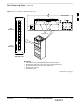
BTS Redundancy/Alarm Testing – continued Power Supply Redundancy Follow the steps in Table 3-47 to verify redundancy of the power supply modules. Alarms reported by the master GLI (displayed via the alarm monitor) are also verified.
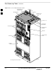
3-88 CCD–1 CCD–2 PS–2 CSM–2 PS–6 GLI2–2 GLI2–1 MCC24–7 MCC24–1 MCC24–8 MCC24–2 MCC24–9 MCC24–3 MCC24–10 MCC24–4 MCC24–11 MCC24–5 MCC24–12 MCC24–6 BBX2–7 BBX2–1 BBX2–8 BBX2–2 BBX2–9 BBX2–3 BBX2–10 BBX2–4 BBX2–11 BBX2–5 FAN MODULE PWR/ALM 1B 3B 2D 1A 30 30 2B 30 4B 3D 4D 3C 30 4C 30 4A 30 L 2C P A 3A 1D CIO 2A 30 BBX2–R 1C 30 BBX2–6 Switch 68P09253A61 SCt4812T CDMA BTS Optimization/ATP PS–9 REAR FRONT PS–8 AMR–1 AMR–2 MPC/EMPC–1 MPC/EMPC–2 PS–3 38 mm Filler Panel PS
BTS Redundancy/Alarm Testing – continued Miscellaneous Alarm/Redundancy Tests Follow the steps in Table 3-48 to verify alarms reported by the master GLI are displayed via the alarm monitor if a BTS frame module failure occurs. Table 3-48: Miscellaneous Alarm Tests Step Action 1 Select Util>Alarm Monitor to display the alarm monitor window. 2 Perform the following to verify fan module alarms: • Unseat a fan module (see Figure 3-21 or Figure 3-22).
BTS Redundancy/Alarm Testing – continued Figure 3-21: +27 V BTS C-CCP Fan Modules LATCHES FAN MODULE REAR FAN MODULE REAR REAR PWR/ALM FRONT 3 FAN MODULE PWR/ALM FRONT PWR/ALM FRONT FAN MODULES FW00130 Figure 3-22: –48 V BTS C-CCP and Power Conversion Shelf Fan Modules LATCHES FAN MODULE REAR FRONT FAN MODULE REAR PWR/ALM FRONT FAN MODULE REAR PWR/ALM FRONT PWR/ALM FAN MODULES LATCHES FAN MODULE REAR FRONT FAN MODULE REAR PWR/ALM FRONT PWR/ALM FW00489 FAN MODULES 3-90 SCt48
BTS Redundancy/Alarm Testing – continued BBX Redundancy Follow the steps in Table 3-49 to verify redundancy of the BBXs in the C–CCP shelf. Alarms reported by the master GLI (displayed via the alarm monitor) are also verified. This test can be repeated for additional sectors at the customer’s discretion. Table 3-49: BBX Redundancy Alarms Step Action 3 n WARNING Any BBXs enabled will immediately key-up.
BTS Redundancy/Alarm Testing – continued CSM, GPS, & LFR/HSO Redundancy/Alarm Tests Follow the procedure in Table 3-50 to verify the manual redundancy of the CSM, GPS, and LFR/HSO boards. Verification of alarms reported is also covered. IMPORTANT * 3 DO NOT perform the procedure in Table 3-50, unless the site is configured with a LORAN–C or HSO timebase as a backup for the GPS. Table 3-50: CSM, GPS, & LFR/HSO, Redundancy/Alarm Tests Step Action n WARNING Any BBXs enabled will immediately key-up.
BTS Redundancy/Alarm Testing – continued Table 3-50: CSM, GPS, & LFR/HSO, Redundancy/Alarm Tests Step 8 Action Allow the CSM 2 board to go INS_ACT. Verify the BBXs are dekeyed and OOS, and the MCCs are OOS_RAM. Verify no other modules went OOS due to the transfer to CSM 2 reference. Observe the PWR/ALM LEDs on CSM 2 front panels are steady GREEN. 3 NOTE It can take up to 20 minutes for the CSM to re-establish the GPS link and go INS. MCCs go OOS_RAM.
BTS Redundancy/Alarm Testing – continued Figure 3-23: +27 V SC 4812T Starter Frame I/O Plate REAR SPAN I/O A RGPS SPAN I/O A SITE I/O 1B 2A SPAN I/O B LFR/ HSO 2 5 3 6 2B GND RX 3A 3B 4A 4B 5A 5B 6A 6B LIVE TERMINALS RGD 3 1A +27 VDC ALARM A 4 LIVE TERMINALS ÄÄÄÄÄÄÄÄÄÄÄÄÄÄÄÄÄÄÄ ÄÄÄÄÄÄÄÄÄÄÄÄÄÄÄÄÄÄÄ ÄÄÄÄÄÄÄÄÄÄÄÄÄÄÄÄÄÄÄ ÄÄÄÄÄÄÄÄÄÄÄÄÄÄÄÄÄÄÄ ÄÄÄÄÄÄÄÄÄÄÄÄÄÄÄÄÄÄÄ ÄÄÄÄÄÄÄÄÄÄÄÄÄÄÄÄÄÄÄ ÄÄÄÄÄÄÄÄÄÄÄÄÄÄÄÄÄÄÄ ÄÄÄÄÄÄÄÄÄÄÄÄÄÄÄÄÄÄÄ ÄÄÄÄÄÄÄÄÄÄÄÄÄÄÄÄÄÄÄ ÄÄÄÄÄÄÄÄÄÄÄÄÄÄÄÄÄÄÄ ÄÄÄÄÄÄÄÄÄÄÄÄÄÄÄÄÄÄÄ ÄÄÄÄ
BTS Redundancy/Alarm Testing – continued LPA Redundancy Test Follow the procedure in Table 3-51 to verify redundancy of the LPAs. WARNING First verify there are no BBX channels keyed BEFORE moving the antenna connection. Failure to do so can result in serious personal injury and/or equipment damage.
BTS Redundancy/Alarm Testing – continued MGLI/GLI Redundancy Test CAUTION This test can only be performed when the MM path is established by the MM (not just with LAPD link connected). Attempting to force the GLIs to “hot swap” under alarm monitor control, when isolated from the MM, causes MGLIs to hang up.
BTS Alarms Testing Alarm Test Overview ALARM connectors provide Customer Defined Alarm Inputs and Outputs. The customer can connect BTS site alarm input sensors and output devices to the BTS, thus providing alarm reporting of active sensors as well controlling output devices. The SC 4812T is capable of concurrently monitoring 36 input signals coming into the BTS. These inputs are divided between 2 Alarm connectors marked ‘ALARM A’ and ‘ALARM B’ located at the top of the frame (see Figure 3-24).
BTS Alarms Testing – continued Figure 3-24: Alarm Connector Location and Connector Pin Numbering ÂÂÂÂÂÂ ÂÂÂÂÂÂ ÂÂÂÂÂÂ ÂÂÂÂÂÂ ÂÂÂÂÂÂ Á ÁÁ Á Á 3 1 1 2 2 59 59 60 60 FW00301 Purpose The following procedures verify the customer defined alarms and relay contacts are functioning properly. These tests are performed on all AMR alarms/relays in a sequential manner until all have been verified. Perform these procedures periodically to ensure the external alarms are reported properly.
BTS Alarms Testing – continued NOTE Abbreviations used in the following figures and tables are defined as: NC = normally closed NO = normally open COM or C = common CDO = Customer Defined (Relay) Output CDI = Customer Defined (Alarm) Input 3 Figure 3-25: AMR Connector Pin Numbering A CDI 18 ... A CDI 1 Returns 60 26 2 60 26 59 25 1 59 25 ALARM A (AMR 1) Returns 2 1 ALARM B (AMR 2) B CDI 36 ...
BTS Alarms Testing – continued Table 3-53: CDI Alarm Input Verification Using the Alarms Test Box Step 3 Action 3 Click on the Device menu. 4 Click on the Customer Alarm Inputs menu item. 5 Click on N.O. Inputs. A status report window displays the results of the action. 6 Click on the OK button to close the status report window. 7 Set all switches on the alarms test box to the Open position. 8 Connect the alarms test box to the ALARM A connector (see Figure 3-24).
BTS Alarms Testing – continued Table 3-53: CDI Alarm Input Verification Using the Alarms Test Box Step Action 26 Connect the alarms test box to the ALARM B connector. A clear alarm should be reported for alarm inputs 19 through 36. 27 Set all switches on the alarms test box to the Open position. An alarm should be reported for each switch setting. 28 Set all switches on the alarms test box to the Closed position. A clear alarm should be reported for each switch setting.
BTS Alarms Testing – continued CDI Alarm Input Verification without Alarms Test Box Table 3-54 describes how to test the CDI alarm input verification without the use of the Alarms Test Box. Follow the steps as instructed and compare results with the LMF display. NOTE 3 It may take a few seconds for alarms to be reported. The default delay is 5 seconds. When shorting alarm pins wait for the alarm report before removing the short.
BTS Alarms Testing – continued Table 3-54: CDI Alarm Input Verification Without the Alarms Test Box Step Action 14 Refer to Figure 3-25 and sequentially short the ALARM A connector CDI 1 through CDI 18 pins (25–26 through 59–60) together. A clear alarm should be reported for each pair of pins that are shorted. An alarm should be reported for each pair of pins when the short is removed.
BTS Alarms Testing – continued Table 3-55: Pin and Signal Information for Alarm Connectors ALARM A Pin 3 Signal Name ALARM B Pin Signal Name Pin Signal Name Pin Signal Name 7 A CDO3 NC 37 Cust Retn 7 7 B CDO11 NC 37 B CDI 25 8 A CDO3 Com 38 A CDI 7 8 B CDO11 Com 38 Cust Retn 25 9 A CDO3 NO 39 Cust Retn 8 9 B CDO11 NO 39 B CDI 26 10 A CDO4 NC 40 A CDI 8 10 B CDO12 NC 40 Cust Retn 26 11 A CDO4 Com 41 Cust Retn 9 11 B CDO12 Com 41 B CDI 27 12 A CDO4 NO 42 A
Chapter 4: Automated Acceptance Test Procedure (ATP) Table of Contents Mar 2001 Automated Acceptance Test Procedures – All–inclusive TX & RX . . . . . . . . . Introduction . . . . . . . . . . . . . . . . . . . . . . . . . . . . . . . . . . . . . . . . . . . . . . ATP Test Prerequisites . . . . . . . . . . . . . . . . . . . . . . . . . . . . . . . . . . . . . . TX OUT Connection . . . . . . . . . . . . . . . . . . . . . . . . . . . . . . . . . . . . . . . ATP Test Procedure . . . . . . . . . . . . . . . .
Table of Contents – continued Notes 4 SCt4812T CDMA BTS Optimization/ATP Mar 2001 DRAFT