
Specifications
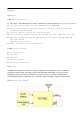
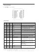
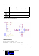
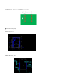

Table Of Contents

1.3 1.
1.
summary..................................................................................................................................................................... 3
1.2 function...............................................................................................................................................3
1.1.1 1.1.1Product characteristics......................................................................................................3
1.1.2 1.1.2Application scenario..........................................................................................................3
1.2 1.2describe.........................................................................................................................................
Catalogue
3
3 Functional
block diagram....................................................................................................................................3
2. 2.
PIN Foot definition............................................................................................................................................... 4
2.1 2.1modelg r o u p PIN Interface diagram.................................................................................4
2.2 2.2Pin function................................................................................................................................. 4
3. 3.
Module characteristics and specifications..................................................................................................5
3.1 3.1WiFi RF specification.................................................................................................................5
3.2 3.2BLE RF specification...................................................................................................................5
3.3 3.3Module electrical parameters................................................................................................6
4. 4.
Reference application and PCB Layout........................................................................................................ 6
4.1 4.1Application schematic reference......................................................................................... 6
4.2 4.2PCB Layout reference resources.......................................................................................... 6
5.5.
reference resources PCB encapsulation......................................................................................................... 7
5.1 5.1Package size: .............................................................................................................................. 7
5.2 5.2Recommended pads.................................................................................................................7
6.6.
Revision history.................................................................................................................................................... 8