
Data Sheet

Nexperia
74HC595-Q100; 74HCT595-Q100
8-bit serial-in, serial or parallel-out shift register with output latches; 3-state
74HC_HCT595_Q100 All information provided in this document is subject to legal disclaimers. © Nexperia B.V. 2017. All rights reserved.
Product data sheet Rev. 3 — 28 February 2017
4 / 23
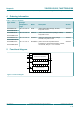
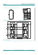
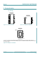
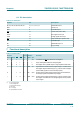
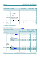
6 Pinning information
6.1 Pinning
74HC595-Q100
74HCT595-Q100
Q1 V
CC
Q2 Q0
Q3 DS
Q4 OE
Q5 STCP
Q6 SHCP
Q7 MR
GND Q7S
aaa-003476
1
2
3
4
5
6
7
8
10
9
12
11
14
13
16
15
Figure 5. Pin configuration for SO16
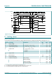
74HC595-Q100
74HCT595-Q100
Q1 V
CC
Q2 Q0
Q3 DS
Q4 OE
Q5 STCP
Q6 SHCP
Q7 MR
GND Q7S
aaa-003477
1
2
3
4
5
6
7
8
10
9
12
11
14
13
16
15
Figure 6. Pin configuration for (T)SSOP16
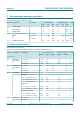
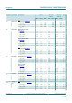
aaa-003478
74HC595-Q100
74HCT595-Q100
Q7 MR
Q6 SHCP
Q5 STCP
Q4 OE
Q3 DS
Q2 Q0
GND
Q7S
Q
1
V
C
C
Transparent top view
7 10
6 11
5 12
4 13
3 14
2 15
8
9
1
16
terminal 1
index area
GND
(1)
(1) This is not a supply pin. The substrate is attached to this pad using conductive die attach material. There is no
electrical or mechanical requirement to solder this pad. However, if it is soldered, the solder land should remain floating or
be connected to GND.
Figure 7. Pin configuration for DHVQFN16