
Data Sheet

Nexperia
74HC595-Q100; 74HCT595-Q100
8-bit serial-in, serial or parallel-out shift register with output latches; 3-state
74HC_HCT595_Q100 All information provided in this document is subject to legal disclaimers. © Nexperia B.V. 2017. All rights reserved.
Product data sheet Rev. 3 — 28 February 2017
12 / 23
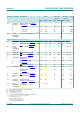
V
CC
= supply voltage in V.
[6] All 9 outputs switching.
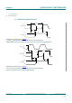
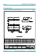
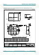
11.1 Waveforms and test circuit
mna557
SHCP input
Q7S output
t
PLH
t
PHL
t
W
1/f
max
V
M
V
OH
V
I
GND
V
OL
V
M
Measurement points are given in Table 8.
V
OL
and V
OH
are typical output voltage levels that occur with the output load.
Figure 9. Shift clock pulse, maximum frequency and input to output propagation delays
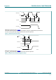
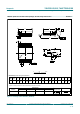
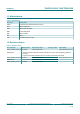
mna558
STCP input
Qn output
t
PLH
t
PHL
t
W
t
su
1/f
max
V
M
V
OH
V
I
GND
V
OL
V
M
SHCP input
V
I
GND
V
M
Measurement points are given in Table 8.
V
OL
and V
OH
are typical output voltage levels that occur with the output load.
Figure 10. Storage clock to output propagation delays