
Data Sheet

©
Nexperia B.V. 2017. All rights reserved
74HC_HCT00 All information provided in this document is subject to legal disclaimers.
Product data sheet Rev. 7 — 25 November 2015 2 of 15
Nexperia
74HC00; 74HCT00
Quad 2-input NAND gate
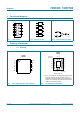
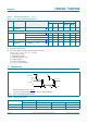
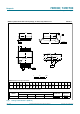
4. Functional diagram
5. Pinning information
5.1 Pinning
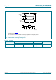
Fig 1. Logic symbol Fig 2. IEC logic symbol Fig 3. Logic diagram (one gate)
PQD
$
<
%
$
<
%
$
<
%
$
<
%
PQD
PQD
$
%
<
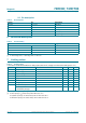
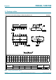
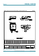
(1) This is not a supply pin. The substrate is attached to this
pad using conductive die attach material. There is no
electrical or mechanical requirement to solder this pad.
However, if it is soldered, the solder land should remain
floating or be connected to GND.
Fig 4. Pin configuration SO14 and (T)SSOP14 Fig 5. Pin configuration DHVQFN14
+&
+&7
$ 9
&&
% %
< $
$ <
% %
< $
*1' <
DDO
DDO
+&
+&7
*1'
7UDQVSDUHQWWRSYLHZ
< $
% %
$ <
< $
% %
*1'
<
$
9
&&
WHUPLQDO
LQGH[DUHD