
User's Manual
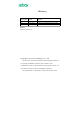
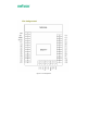

Pin Description
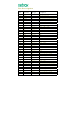
Pin
NO.
Pin name Pin type Description
1
GND Ground GND
2
/RST
I
Active low chip reset
3
SWDIO I/O Programming and debug interface
4
SWCLK I/O Programming and debug interface
5
VCC Power 2.1V-3.6V DC power supply
6
PA0 Digital I/O
GPIO
7
PB2 Digital I/O
GPIO / MI / RXD / MSCL
8
PB1 Digital I/O
GPIO / MO / TXD / MSDA
9
PB3 Digital I/O
GPIO / CLK / nCTS
10
PB4 Digital I/O
GPIO / SS / nRTS
11
PB0 Digital I/O
GPIO / IRQA
12
PC0 Digital I/O
GPIO / IRQD
13
PA1 Digital I/O
GPIO
14 GND Ground GND
15 GND Ground GND
16 GND Ground GND
17
PA2 Digital I/O
GPIO
18
PB7 Digital I/O
GPIO / IRQC
19
PB6 Digital I/O
GPIO / IRQB
20
PA4 Digital I/O
GPIO / ADC0
21
PA5 Digital I/O
GPIO / ADC1
22
PC1 Digital I/O
GPIO / ADC2
23
PB5 Digital I/O
GPIO / ADC3
24
PA6 Digital I/O
GPIO
25
PA3 Digital I/O
GPIO
26
VCC Power 2.1V-3.6V DC power supply
27
VCC Power 2.1V-3.6V DC power supply
28
NC
No
Connection
29
PA4 Digital I/O
GPIO / ADC0
30
PA5 Digital I/O
GPIO / ADC1
31
PC0 I/O Programming and debug interface
32
SWCLK/JCLK I/O Programming and debug interface
33
PC2 I/O Programming and debug interface
34
PC3 I/O Programming and debug interface
35
PC4/SWDIO
I/O Programming and debug interface
36
/RST
I
Active low chip reset
37
VCC Power 2.1V-3.6V DC power supply
38
GND Ground GND