
Mos Integrated Circuit Data Sheet


µ
PD75P3116
9
Data Sheet U11369EJ3V0DS
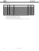
3.2 Non-Port Pins (1/2)
Pin Name I/O Alternate Function Status I/O Circuit
Function After Reset Type
Note 1
TI0 Input P13 External event pulse input to timer/event counter Input <B>-C
TI1 P12/INT2/TI2
TI2 P12/INT2/TI1
PTO0 Output P20 Timer/event counter output Input E-B
PTO1 P21
PTO2 P22/PCL
PCL P22/PTO2 Clock output
BUZ P23 Frequency output (for buzzer or system clock trimming)
SCK I/O P01 Serial clock I/O Input <F>-A
SO/SB0 P02 Serial data output <F>-B
Serial data bus I/O
SI/SB1 P03 Serial data input <M>-C
Serial data bus I/O
INT4 Input P00 Edge detection vectored interrupt input <B>
(valid for detecting both rising and falling edges)
INT0 Input P10 Edge detection vectored interrupt
With noise eliminator/
Input <B>-C
input (detection edge is selectable) asynchronous is
INT0/P10 can be used to select a selectable
INT1 P11
noise eliminator.
Asynchronous
INT2 Input P12/TI1/TI2 Rising edge detection testable input Asynchronous
KR0 to KR3 I/O P60 to P63 Parallel falling edge detection testable input Input <F>-A
X1 Input — Ceramic/crystal resonator connection for main system — —
clock oscillation. If using an external clock, input the signal
X2 —
to X1 and input the inverted signal to X2.
XT1 Input — Crystal resonator connection for subsystem clock oscillation. — —
If using an external clock, input the signal to XT1 and input
XT2 —
the inverted signal to XT2. XT1 can be used as a 1-bit (test)
input.
RESET Input — System reset input (low-level active) — <B>
MD0 to MD3 Input P30 to P33 Mode selection for program memory (PROM) write/verify Input E-B
D0 to D3 I/O
P60/KR0 to P63/KR3
Data bus for program memory (PROM) write/verify Input <F>-A
D4 to D7 P50 to P53 M-E
VPP
Note 2
— — Programmable power supply voltage applied for program — —
memory (PROM) write/verify.
During normal operation, connect directly to VDD.
Apply +12.5 V for PROM write/verify.
VDD — — Positive power supply — —
Vss — — Ground potential — —
Notes 1. Circuit types enclosed in angle brackets indicate Schmitt-triggered input.
2. The V
PP pin does not operate correctly when it is not connected to the VDD pin during normal operation.