
Mos Integrated Circuit Data Sheet


µµ
µµ
µ
PD75P3116
38
Data Sheet U11369EJ3V0DS
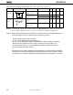
Serial Transfer Operation
2-wire and 3-wire serial I/O mode (SCK...Internal clock output): (T
A = –40 to +85˚C, VDD = 1.8 to 5.5 V)
Parameter Symbol Test Conditions MIN. TYP. MAX. Unit
SCK cycle time t
KCY1 VDD = 2.7 to 5.5 V 1300 ns
V
DD = 1.8 to 5.5 V 3800 ns
SCK high-/low-level t
KL1, tKH1 VDD = 2.7 to 5.5 V
tKCY1/2–50
ns
width V
DD = 1.8 to 5.5 V
tKCY1/2–150
ns
SI
Note 1
setup time tSIK1 VDD = 2.7 to 5.5 V 150 ns
(to SCK↑)VDD = 1.8 to 5.5 V 500 ns
SI
Note 1
hold time tKSI1 VDD = 2.7 to 5.5 V 400 ns
(from SCK↑)V
DD = 1.8 to 5.5 V 600 ns
SO
Note 1
output delay tKSO1 RL = 1 kΩ,VDD = 2.7 to 5.5 V 0 250 ns
time from SCK↓ CL = 100 pF
Note 2
VDD = 1.8 to 5.5 V 0 1000 ns
Notes 1. In 2-wire serial I/O mode, read this parameter as SB0 or SB1 instead.
2. R
L and CL are the load resistance and load capacitance of the SO output lines, respectively.
2-wire and 3-wire serial I/O mode (SCK...External clock input): (TA = –40 to +85˚C, VDD = 1.8 to 5.5 V)
Parameter Symbol Test Conditions MIN. TYP. MAX. Unit
SCK cycle time tKCY2 VDD = 2.7 to 5.5 V 800 ns
VDD = 1.8 to 5.5 V 3200 ns
SCK high-/low-level tKL2, tKH2 VDD = 2.7 to 5.5 V 400 ns
width VDD = 1.8 to 5.5 V 1600 ns
SI
Note 1
setup time tSIK2 VDD = 2.7 to 5.5 V 100 ns
(to SCK↑)VDD = 1.8 to 5.5 V 150 ns
SI
Note 1
hold time tKSI2 VDD = 2.7 to 5.5 V 400 ns
(from SCK↑)VDD = 1.8 to 5.5 V 600 ns
SO
Note 1
output delay tKSO2 RL = 1 kΩ,VDD = 2.7 to 5.5 V 0 300 ns
time from SCK↓ CL = 100 pF
Note 2
VDD = 1.8 to 5.5 V 0 1000 ns
Notes 1. In 2-wire serial I/O mode, read this parameter as SB0 or SB1 instead.
2. RL and CL are the load resistance and load capacitance of the SO output lines, respectively.