
Mos Integrated Circuit Data Sheet


µµ
µµ
µ
PD75P3116
36
Data Sheet U11369EJ3V0DS
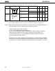
DC Characteristics (TA = –40 to +85˚C, VDD = 1.8 to 5.5 V)
Parameter Symbol Test Conditions MIN. TYP. MAX. Unit
LCD drive voltage VLCD VAC0 = 0 TA = –40 to +85°C 2.7 VDD V
T
A = –10 to +85°C 2.2 VDD V
VAC0 = 1 1.8 V
DD V
VAC current
Note 1
IVAC VAC0 = 1, VDD = 2.0 V ±10% 1 4
µ
A
LCD output voltage VODC lo = ±1.0
µ
AVLCD0 = VLCD 0 ±0.2 V
deviation
Note 2
(common)
VLCD1 = VLCD × 2/3
LCD output voltage VODS lo = ±0.5
µ
A
VLCD2 = VLCD × 1/3
0 ±0.2 V
deviation
Note 2
(segment) 1.8 V ≤ VLCD ≤ VDD
Supply current
Note 3
IDD1 6.00 MHz
Note 4
VDD = 5.0 V ±10%
Note 5
3.2 9.5 mA
Crystal oscillation
VDD = 3.0 V ±10%
Note 6
0.55 1.6 mA
I
DD2
C1 = C2 = 22 pF
HALT mode VDD = 5.0 V ±10% 0.7 2.0 mA
V
DD = 3.0 V ±10% 0.25 0.8 mA
IDD1 4.19 MHz
Note 4
VDD = 5.0 V ±10%
Note 5
2.5 7.5 mA
Crystal oscillation
VDD = 3.0 V ±10%
Note 6
0.45 1.35 mA
IDD2
C1 = C2 = 22 pF
HALT mode VDD = 5.0 V ±10% 0.65 1.8 mA
VDD = 3.0 V ±10% 0.22 0.7 mA
IDD3 32.768 kHz
Note 7
Low-voltage VDD = 3.0 V ± 10% 45 130
µ
A
Crystal oscillation
mode
Note 8
VDD = 2.0 V ±10% 20 55
µ
A
V
DD
= 3.0 V, T
A
= 25˚C
45 90
µ
A
VDD = 3.0 V ±10% 42 120
µ
A
V
DD
= 3.0 V, T
A
= 25˚C
42 85
µ
A
IDD4 HALT mode
V
DD
= 3.0 V ±10%
5.5 18
µ
A
V
DD
= 2.0 V ±10%
2.2 7
µ
A
VDD = 3.0 V, TA = 25˚C
5.5 12
µ
A
VDD = 3.0 V ±10%
4.0 12
µ
A
V
DD
= 3.0 V,
4.0 8
µ
A
TA = 25˚C
IDD5 XT1 = 0 V
Note 10
VDD = 5.0 V ±10% 0.05 10
µ
A
STOP mode VDD = 3.0 V TA = –40 to +85˚C 0.02 5
µ
A
±10%
TA = 25˚C 0.02 3
µ
A
Notes 1. Set to VAC0 = 0 when the low current consumption mode and the stop mode are used. If VAC0 = 1
is set, the current increases for approx. 1
µ
A.
2. The voltage deviation is the difference from the output voltage corresponding to the ideal value of the
segment and common outputs (VLCDn; n = 0, 1, 2).
3. Not including currents flowing through on-chip pull-up resistors.
4. Including oscillation of the subsystem clock.
5. When the processor clock control register (PCC) is set to 0011 and the device is operated in the high-
speed mode.
6. When PCC is set to 0000 and the device is operated in the low-speed mode.
7. When the system clock control register (SCC) is set to 1001 and the device is operated on the
subsystem clock, with main system clock oscillation stopped.
8. When the sub-oscillator control register (SOS) is set to 0000.
9. When SOS is set to 0010.
10. When SOS is set to 00×1 and the feedback resistor of the sub-oscillator is not used (×: Don’t care).
Low current
consumption
mode
Note 9
Low-
voltage
mode
Note 8
Low
current
consump-
tion mode
Note 9