
Mos Integrated Circuit Data Sheet


µµ
µµ
µ
PD75P3116
33
Data Sheet U11369EJ3V0DS
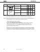
Main System Clock Oscillator Characteristics (TA = –40 to +85°C, VDD = 1.8 to 5.5 V)
Resonator Recommended Constant Parameter Test Conditions MIN. TYP. MAX. Unit
Ceramic Oscillation 1.0
6.0
Note 2
MHz
resonator frequency (fx)
Note 1
Oscillation After VDD reaches oscil- 4 ms
stabilization time
Note 3
lation voltage range MIN.
Crystal Oscillation 1.0
6.0
Note 2
MHz
resonator frequency (fx)
Note 1
Oscillation VDD = 4.5 to 5.5 V 10 ms
stabilization time
Note 3
VDD = 1.8 to 5.5 V 30
External X1 input 1.0
6.0
Note 2
MHz
clock frequency (fx)
Note 1
X1 input 83.3 500 ns
high-/low-level width
(t
XH, tXL)
Notes 1. Indicates only oscillator characteristics. Refer to AC Characteristics for instruction execution time.
2. When the power supply voltage is 1.8 V ≤ V
DD < 2.7 V and the oscillation frequency is 4.19 MHz < fx
≤ 6.0 MHz, setting the processor clock control register (PCC) to 0011 makes 1 machine cycle less than
the required 0.95
µ
s. Therefore, set PCC to a value other than 0011.
3. The oscillation stabilization time is necessary for oscillation to stabilize after applying V
DD or releasing
the STOP mode.
Caution When using the main system clock oscillator, wire as follows in the area enclosed by the broken
lines in the above figures to avoid an adverse effect from wiring capacitance.
• Keep the wiring length as short as possible.
• Do not cross the wiring with the other signal lines.
• Do not route the wiring near a signal line through which a high fluctuating current flows.
• Always make the ground point of the oscillator capacitor the same potential as V
DD.
• Do not ground the capacitor to a ground pattern through which a high current flows.
• Do not fetch signals from the oscillator.
X2
X1
C1
C2
V
DD
X2
X1
C1
C2
V
DD
X1
X2