
Mos Integrated Circuit Data Sheet


µµ
µµ
µ
PD75P3116
32
Data Sheet U11369EJ3V0DS
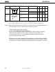
9. ELECTRICAL SPECIFICATIONS
Absolute Maximum Ratings (TA = 25˚C)
Parameter Symbol Test Conditions Rating Unit
Power supply voltage VDD –0.3 to +7.0 V
PROM power supply V
PP –0.3 to +13.5 V
voltage
Input voltage V
I1 Except port 5 –0.3 to VDD + 0.3 V
VI2 Port 5 (N-ch open drain) –0.3 to +14 V
Output voltage V
O –0.3 to VDD + 0.3 V
Output current, high I
OH Per pin –10 mA
Total of all pins –30 mA
Output current, low IOL Per pin 30 mA
Total of all pins 220 mA
Operating ambient TA –40 to +85
Note
˚C
temperature
Storage temperature Tstg –65 to +150 ˚C
Note When LCD is driven in normal mode: TA = –10 to +85˚C
Caution Product quality may suffer if the absolute maximum rating is exceeded even momentarily for any
parameter. That is, the absolute maximum ratings are rated values at which the product is on
the verge of suffering physical damage, and therefore the product must be used under conditions
that ensure that the absolute maximum ratings are not exceeded.
Capacitance (T
A = 25˚C, VDD = 0 V)
Parameter Symbol Test Conditions MIN. TYP. MAX. Unit
Input capacitance CIN f = 1 MHz 15 pF
Output capacitance COUT Unmeasured pins returned to 0 V. 15 pF
I/O capacitance CIO 15 pF