
User's Manual
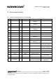
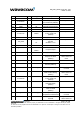
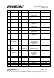
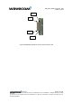
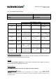
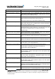
Table Of Contents
- General description
- Interfaces
- General Purpose Connector (GPC)
- Power supply
- Electrical information for digital I/O
- LCD interface
- SPI Auxiliary bus
- Keyboard interface
- Main serial link (UART1)
- Auxiliary serial link (UART2)
- SIM interface
- General Purpose Input/Output
- Activity status indication
- Analog to Digital Converter (ADC)
- Audio interface
- Battery charging interface
- ON / ~OFF
- BOOT (optional)
- Reset signal (~RST)
- External Interrupt (~INTR)
- VCC output
- Real Time Clock Supply (VCC_RTC)
- RF interface
- Technical specifications
- Appendix

WM_PRJ_Q2400_PTS_002 - 004
March 5, 2004
3 Technical specifications
3.1 General Purpose Connector pin out description
Pin # Name I/O I/O type Description Comment
1 CHG_IN I Supply Supply for battery
charging
High current
2 CHG_IN I Supply Supply for battery
charging
High current
3 SIM_CLK O 2 X Clock for SIM interface
4 CHG_IN I Supply Supply for battery
charging
High current
5 SIM_RST O 2 X Reset for SIM interface
6 ON/~OFF I CMOS Power ON/OFF control
7 SIM_DATA I/O CMOS / 3X I/O for SIM interface
8 SDA/SPI_IO I/O CMOS/1X Wire interface or SPI
Serial Data
9 SIM_VCC O Supply SIM card supply 6 mA max
10 SCL/SPI_CLK O 1X Wire interface or SPI
Serial clock
11 VDD I Supply Low power supply 3.1 V minimum or
connected to VBATT
12 BOOT I CMOS BOOT
Pull down through 1 KΩ
for Flash downloading
13 ROW0 I/O CMOS/1X Keyboard Row
14 ~RST I/O SCHMITT Module Reset Active low
15 ROW1 I/O CMOS/1X Keyboard Row
16 ~INTR I CMOS External interrupt
Active low. 100 KΩ
Pull-up inside
17 ROW2 I/O CMOS/1X Keyboard Row
18 GPI or
CT103/TXD2 *
I CMOS or 3x General Purpose Input or
Aux.serial Link (UART2)
100K Pull-down inside -
Multiplexed
confidential ©
Page : 42 / 63
This document is the sole and exclusive property of WAVECOM. Not to be distributed or divulged without prior written
agreement.
Ce document est la propriété exclusive de WAVECOM. Il ne peut être communiqué ou divulgué à des tiers sans son
autorisation préalable.