
User's Manual
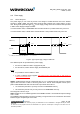
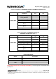
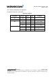
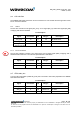
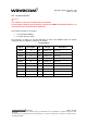
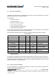
Table Of Contents
- General description
- Interfaces
- General Purpose Connector (GPC)
- Power supply
- Electrical information for digital I/O
- LCD interface
- SPI Auxiliary bus
- Keyboard interface
- Main serial link (UART1)
- Auxiliary serial link (UART2)
- SIM interface
- General Purpose Input/Output
- Activity status indication
- Analog to Digital Converter (ADC)
- Audio interface
- Battery charging interface
- ON / ~OFF
- BOOT (optional)
- Reset signal (~RST)
- External Interrupt (~INTR)
- VCC output
- Real Time Clock Supply (VCC_RTC)
- RF interface
- Technical specifications
- Appendix

WM_PRJ_Q2400_PTS_002 - 004
March 5, 2004
Power consumption in E-GSM/GPRS 900 MHz and GSM/GPRS 850 MHz mode
class 10
Conditions I
NOM
I
MAX
During TX bursts @Pcl5 1.60 A peak 1.8 A peak
During RX bursts
110 mA peak 115 mA peak
Average 1Rx/1Tx @Pcl5 250 mA 300 mA
Average 1Rx/1Tx @Pcl8 190 mA 200 mA
Average GPRS Cl 10 (3Rx/2Tx)
@Pcl5
400 mA 510 mA
Average GPRS Cl 10 (3Rx/2Tx)
@Pcl8
260 mA 300 mA
VBATT+VDD
Average Idle mode 3 mA 7 mA
Power Control Level: Pcl5=2 W typ.; Pcl8=0.5 W typ.
Power consumption in GSM/GPRS 1800 MHz and
GSM/GPRS 1900 MHz mode class 10
Conditions I
NOM
I
MAX
During TX bursts @Pcl0 1 A peak 1.5 A peak
During RX bursts
130 mA peak 140 mA peak
Average 1Rx/1Tx @Pcl0 190 mA 235 mA
Average 1Rx/1Tx @Pcl3 150 mA 180 mA
Average GPRS Cl 10 (3Rx/2Tx)
@Pcl0
320 mA 410 mA
Average GPRS Cl 10 (3Rx/2Tx)
@Pcl3
240 mA 270 mA
VBATT+VDD
Average Idle mode 2 mA 6.5 mA
Power Control Level: Pcl0=1 W typ.; Pcl3=0.25 W typ.
Power Supply Pinout
Signal Pin number
+VBATT
55, 57, 58, 59, 60
VDD
11
GND
Shielding
The ground connection is done through the shielding the four legs have to be soldered to the
ground plane.
confidential ©
Page : 16 / 63
This document is the sole and exclusive property of WAVECOM. Not to be distributed or divulged without prior written
agreement.
Ce document est la propriété exclusive de WAVECOM. Il ne peut être communiqué ou divulgué à des tiers sans son
autorisation préalable.