
User's Manual
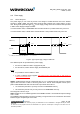
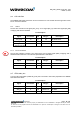
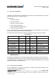
Table Of Contents
- General description
- Interfaces
- General Purpose Connector (GPC)
- Power supply
- Electrical information for digital I/O
- LCD interface
- SPI Auxiliary bus
- Keyboard interface
- Main serial link (UART1)
- Auxiliary serial link (UART2)
- SIM interface
- General Purpose Input/Output
- Activity status indication
- Analog to Digital Converter (ADC)
- Audio interface
- Battery charging interface
- ON / ~OFF
- BOOT (optional)
- Reset signal (~RST)
- External Interrupt (~INTR)
- VCC output
- Real Time Clock Supply (VCC_RTC)
- RF interface
- Technical specifications
- Appendix

WM_PRJ_Q2400_PTS_002 - 004
March 5, 2004
2.2 Power supply
2.2.1 General description
The power supply is one of the key issues in the design of a GSM terminal. Due to the bursted
emission in GSM / GPRS, the power supply must be able to deliver high current peaks in a short
time. During these peaks the ripple (U
ripp
) on the supply voltage must not exceed the limits specified
in table “Power Supply Voltage” hereafter.
In communication mode, a GSM/GPRS class 2 terminal emits 577 µs radio bursts every 4.615 ms.
In communication mode, a GPRS class 10 terminal emits 1154 µs radio bursts every 4.615 ms.
Uripp
Uripp
T = 4.615 ms
t = 577 µs
VBATT
(1 )
IBATT
(1)
or VDD if connected to VBATT
V
max
V
min
Figure 2: Typical power supply voltage in GSM mode
Two different inputs are provided for the power supply:
• the first one, VBATT is used to supply the RF part,
• the second one, VDD is used to supply the baseband part.
Notes
:
• It is possible to connect VBATT to VDD.
• In case of separate power supplies, they have to be in the same state i.e both active or
inactive at the same time.
VBATT: supplies directly the RF components with 3.6 V. It is essential to keep a minimum voltage
ripple at this connection in order to avoid any phase error. The RF Power Amplifier current (2.0 A
peak in GSM /GPRS mode with a 50 Ohms RF output flows with a ratio of:
• 1/8 of the time (around 577 µs every 4.615 ms for GSM/GPRS class 2),
• 2/8 of the time (around 1154 µs every 4.615 ms for GSM/GPRS class 10).
The rising time is around 10 µs.
VDD: supplies the +2.8 V ballast regulators of the WISMO module. It is essential to keep the voltage
over 3.1 volts.
The WISMO module shielding case is the grounding. The ground has to be connected on the mother
board through a complete layer on the PCB.
confidential ©
Page : 14 / 63
This document is the sole and exclusive property of WAVECOM. Not to be distributed or divulged without prior written
agreement.
Ce document est la propriété exclusive de WAVECOM. Il ne peut être communiqué ou divulgué à des tiers sans son
autorisation préalable.