Jupiter 30 / 20 GPS receiver module Integrator’s Manual Related documents •Jupiter Series Development kit guide LA000645 • Navman NMEA reference manual MN000315 • SiRF Binary Protocol reference manual LA000577C © 2006 Navman New Zealand. All rights reserved. Proprietary information and specifications subject to change without notice.
Contents 1.0 Introduction........................................................................................................ 4 2.0 Hardware application information................................................................... 4 2.1 Electrical connections (SMT pad interface)................................................................... 4 2.2 Physical dimensions...................................................................................................... 6 2.
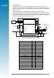
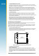
Figures Figure 2-1: Lead-free and tin/lead reflow profile recommendation...................................... 6 Figure 2-2: Sample application circuit................................................................................. 8 Figure 2-3: Recommended application layout dimensions................................................. 9 Figure 2-4: Typical module layout......................................................................................
1.0 Introduction The Navman Jupiter 30 and Jupiter 20 series of GPS receiver modules are complete GPS receivers designed for surface mount assembly (SMT) integration. The modules provide a simple, cost effective GPS solution for application designers. Application integration will vary primarily with respect to antenna system design and EMI protective circuitry. The Jupiter 30 is the successor to the established Jupiter 20, sharing the same form factor (25.4 x 25.4 mm) and electrical compatibility.
Pin No. Name Type 1 PWRIN P main power input (3.
Jupiter 30 Pin Jupiter 20 GPIO Name and Description GPIO Standard & XTrac name DR function 24 13 reserved 6 GPIO (SDO) not connected 25 4 reserved 5 GPIO (SDI) ADC DOut – WAKEUP. push-to-fix wakeup (active on +ve edge) 7 GPIO (SCK) ADC Clk 27 15 ANT_OC. antenna open circuit sensor input (active high) 15 ANT_OC FWD/REV. fwd/rev input (low=forward, high=reverse) 28 1 ANT_CTRL. active antenna control output 1 ANT_CTRL WHEEL_TICKS. wheel tick input 8 14 NANT_SC.
2.3.3 Solder paste mask size This should be adjusted by experimentation according to the customer’s production process requirements. A 1:1 (paste mask:pad size) ratio has been found to be successful. 2.3.4 Solder paste type The module accepts all commonly used solder pastes. The solder paste can be lead based or lead-free.
2.4.3 Decoupling The schematic in Figure 2-2 illustrates a suggested method of decoupling. These are capacitors C1 to C7. This level of decoupling may not be required in a particular application, in which case these capacitors could be omitted. Only the signal lines used in the application require decoupling. All capacitors are highly recommended if the module will experience substantial electromagnetic interference (EMI).
2.4.4 Serial RS232 data level shifter To connect the module to a PC comm. port, the serial data signals must be level shifted to RS232 levels. This has not been shown in the reference design, but many single chip RS232 level shifters are available, such as MAX3232. Note: It is highly recommended to provide test points on the serial data lines and ‘Boot’ signal (pad 3), even if the application circuit does not use these signals.
Ground plane design. We reccomend a complete ground plane is used under the PCB with signal tracks on the same layer as the module. We also recommend having a ground plane on both sides of the PCB underneath the module. If the ground planes are very small, separate analogue and digital ground planes may not be required. The ground return for any signal should have a clear path back to its source and should not mix with other ground return signal paths.
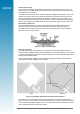
Design of 50 ohm microstrip antenna connection. When designing the signal track from the antenna connection to the antenna input on the module, a controlled impedance microstrip with a characteristic impedance of 50 ohms must be used. The PCB parameters that affect impedance are as follows: 1. Track width (W) 2. PCB substrate thickness (H) 3. PCB substrate permittivity (εr) 4. To a lesser extent, PCB copper thickness (T) and proximity of same layer ground plane.
• be interfaced to a coaxial connector if an external antenna is used • have maximum clearance to ground on the same layer, or at least be half the substrate thickness • be routed away from noise sources such as: switching power supplies, digital signals, oscillators and transmitters The PCB track connection to the RF antenna input must NOT have: • vias • sharp bends • components overlaying the track 2.6 Antenna system design choices 2.6.
2.6.3 Passive antenna A passive antenna does not require any power because it has no amplifier. This is not the best choice if signal strength is a concern, however, it may be sufficient if the signal path is kept to a minimum (usually below 300 mm). An advantage to using a passive antenna is the ability to mount directly onto the application.
2.6.5 DC supply protection for an active antenna Antenna DC supply current limit. When the Jupiter receiver is used with an external active antenna, the DC supply in the coax cable is vulnerable to over-current if a fault occurs in the antenna or its cable gets crushed, for example in a car door. WARNING It is important to note that the module antenna power feed does not have internal current limiting.
Antenna short/open sense inputs and control output. The Jupiter receiver has a digital input to provide signalling when an antenna fault has occurred. These functions are shared with the Jupiter 30 GPIO pads as shown in Table 2-7.
2.7 Jupiter adapter printed circuit board The module supplied in the Development kit is mounted on a carrier PCB in a method typical of a customer application. This carrier PCB illustrates and implements many of the design considerations discussed in this document. The module is interfaced through two separate 20‑pin data connectors with different header pitches. This is for development purposes and provides a simple way to evaluate the surface mount module.
Refer to Table 2-8 for a description of the connector interfaces. Jupiter function J2 (2.54 mm pitch header) pin no. J1 (2 mm pitch header) pin no.
3.2.1 Adaptive TricklePower mode In Adaptive TricklePower mode, the processor automatically returns to full power when signal levels are below the level at which they can be tracked in TricklePower mode. This is the default behaviour when TricklePower is active. Adaptive TricklePower is always enabled on the Jupiter 30 and Jupiter 20 S (XTrac), and selectable on the Jupiter 20 standard module. 3.2.2 Push-to-Fix mode Unlike TricklePower, the operation in this mode is not cyclic.
Unused messages Input messages where the message ID is not between 100 and 255, or where the message ID does not correspond to a specified function, result in the response: $PTTK,INVALID*CS Errors Errors in message receipt (other than checksum errors) result in the response: $PTTK,ERROR,xx*CS where xx is a hexadecimal error code. Magnetic Variation (Declination) The Jupiter 20 module calculates the magnetic variation (the Jupiter 30 does not).
3.4 Navman proprietary NMEA low power mode messages Navman has added a number of proprietary NMEA input messages to configure the TricklePower and Push-To-Fix modes. 3.4.
Bit Pad function Pin (LSB) 0 GPIO15/Fwd-Rev 27 1 GPIO1/Wheel Tick 28 2 GPIO3/Gyro In 8 3 GPIO5/SDI 25 4 GPIO6/SDO 24 5 GPIO7/SCLK 26 6 GPIO9/1PPS 29 (MSB) 7 GPIO10/GPS Fix 23 Table 3-3: Pin configuration of the GPIO lines On the Jupiter 20 D, there is no control of GPIO15, GPIO1, GPIO3, GPIO5, GPIO6 or GPIO7, and all references to these pins are ignored. In each of the messages described in the following sections, x represents a hexadecimal digit. 3.5.
3.7 Antenna power monitor messages The Jupiter software includes antenna monitor messages driven by the state of the antenna monitor inputs. The inputs NANT_SC (short circuit detect – active low) and ANT_OC (open circuit detect – active high) are configured as inputs, and ANT_CTRL (active antenna control) is configured as an output. If the function of any of these pins is overridden using the procedure described in Section 3.6, then this feature is disabled.
4.0 Glossary and acronyms EMI: Electromagnetic Interference FR4 substrate: Flame Retardant type 4. The usual base material from which plated-through-hole and multi-layer printed circuit boards are constructed. The type ‘4’ indicates woven glass reinforced epoxy resin. GPS: Global Positioning System. A space-based radio positioning system that provides accurate position, velocity, and time data.