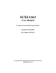
SCXI-1163 User Manual 32-Channel Isolated Digital Output Module September 1994 Edition Part Number 320576-01 © Copyright 1993, 1994 National Instruments Corporation. All Rights Reserved.
National Instruments Corporate Headquarters 6504 Bridge Point Parkway Austin, TX 78730-5039 (512) 794-0100 Technical support fax: (800) 328-2203 (512) 794-5678 Branch Offices: Australia (03) 879 9422, Austria (0662) 435986, Belgium 02/757.00.
Limited Warranty The SCXI-1163 is warranted against defects in materials and workmanship for a period of one year from the date of shipment, as evidenced by receipts or other documentation. National Instruments will, at its option, repair or replace equipment that proves to be defective during the warranty period. This warranty includes parts and labor.
Contents About This Manual .............................................................................................................xi Organization of This Manual .........................................................................................xi Conventions Used in This Manual .................................................................................xii Related Documentation ..................................................................................................
Contents Chapter 4 Register Descriptions .........................................................................................................4-1 Register Description.......................................................................................................4-1 Register Description Format ..............................................................................4-1 SCXI-1163 Registers .........................................................................................
Contents Appendix E SCXI-1163 Cabling .............................................................................................................E-1 SCXI-1340 Cable Assembly ..........................................................................................E-1 SCXI-1340 Installation ......................................................................................E-3 SCXI-1341 Lab-NB, Lab-PC, or Lab-PC+ and SCXI-1344 Lab-LC Cable Assembly .......................................................
Contents Figures Figure 1-1. SCXI-1163 Digital Output Module....................................................................1-1 Figure Figure Figure Figure Figure Figure Figure Figure Figure Figure 2-1. 2-2. 2-3. 2-4. 2-5. 2-6. 2-7. 2-8. 2-9. 2-10. SCXI-1163 Parts Locator Diagram ....................................................................2-2 SCXI-1163 Front Connector Pin Assignment ...................................................2-9 SCXI-1326 Parts Locator Diagram ......................
About This Manual This manual describes the electrical and mechanical aspects of the SCXI-1163 and contains information concerning its operation and programming. The SCXI-1163 is a member of the National Instruments Signal Conditioning eXtensions for Instrumentation (SCXI) Series modules for the National Instruments data acquisition plug-in boards. This module provides 32 isolated digital outputs configured in ports of four channels.
About This Manual • The Glossary contains an alphabetical list and description of terms used in this manual, including abbreviations, acronyms, metric prefixes, mnemonics, and symbols. • The Index contains an alphabetical list of key terms and topics in this manual, including the page where you can find each one.
About This Manual Abbreviations, acronyms, metric prefixes, mnemonics, symbols, and terms are listed in the Glossary.
About This Manual Customer Communication National Instruments wants to receive your comments on our products and manuals. We are interested in the applications you develop with our products, and we want to help if you have problems with them. To make it easy for you to contact us, this manual contains comment and configuration forms for you to complete. These forms are in Appendix F, Customer Communication, at the end of this manual.
Chapter 1 Introduction This chapter describes the SCXI-1163; lists the contents of your SCXI-1163 kit; describes the optional software, optional equipment, and custom cables; and explains how to unpack the SCXI-1163 kit. Figure 1-1 shows the SCXI-1163 module. Figure 1-1. SCXI-1163 Digital Output Module The SCXI-1163 is an SCXI module consisting of 32 optically isolated digital outputs. The SCXI-1163 module provides digital signals where common-mode voltages may be present.
Introduction Chapter 1 With the SCXI-1163, you can use the SCXI chassis as a controller in laboratory testing, production testing, and industrial-process monitoring. What You Need To Get Started SCXI-1163 module SCXI-1163 User Manual SCXI chassis Your computer Optional Software This manual contains complete instructions for directly programming the SCXI-1163. You can order separate software packages for controlling the SCXI-1163 from National Instruments.
Chapter 1 Introduction You can also use the SCXI-1163, combined with the NB Series data acquisition boards, with NI-DAQ software for Macintosh. NI-DAQ software for Macintosh, which is shipped with all National Instruments Macintosh data acquisition boards, comes with language interfaces for MPW C, THINK C, Pascal, and Microsoft QuickBASIC. Any language that uses Device Manager Toolbox calls can access NI-DAQ software for Macintosh.
Introduction • Chapter 1 ERNI Components, Inc. (part number 033-273) The mating connector for the SCXI-1163 front connector is a special 48-pin reversed DIN C female connector. National Instruments uses a polarized and keyed connector to prevent inadvertent upside-down connection to the SCXI-1163. The manufacturer part number National Instruments uses for this mating connector is as follows: • ERNI Components, Inc.
Chapter 2 Configuration and Installation This chapter describes the SCXI-1163 jumper configurations, installation of the SCXI-1163 into the SCXI chassis, signal connections to the SCXI-1163, and cable wiring. Module Configuration The SCXI-1163 module consists of five user-configurable jumpers and one reserved jumper as shown in the parts locator diagram, Figure 2-1.
Chapter 2 Configuration and Installation The SCXI-1163 can accept data in two forms–serial and parallel. Serial data is transferred across the SCXIbus using the Serial Peripheral Interface (SPI) protocol. Using serial communication, one data acquisition board that is cabled to one SCXI module in an SCXI system can control the digital communication for all the boards in the system. Parallel data is read from the rear connector and transferred directly to the outputs at the front connector.
Configuration and Installation Chapter 2 Do not operate damaged equipment. The safety protection features built into this module can become impaired if the module becomes damaged in any way. If it is damaged, turn the module off and do not use until service-trained personnel can check its safety. If necessary, return the module to National Instruments for service and repair to ensure that its safety is not compromised. Do not substitute parts or modify equipment.
Chapter 2 Configuration and Installation - Jumper W5 carries the SCXIbus MISO line, after buffering, to the SERDATOUT signal on the rear signal connector. - Jumper W6 selects the primary operating mode, either serial or parallel, and configures the rear connector accordingly. Further configuration of the board is software controlled and is discussed later in this chapter.
Configuration and Installation Chapter 2 Position PAR disconnects SERDATOUT from the SCXIbus MISO line. Use this position when you will connect the module in parallel to a data acquisition board. Using Jumpers W4 and W5 If a module is not connected to a data acquisition board, the positions of jumpers W4 and W5 are irrelevant. Jumpers W4 and W5 give the data acquisition board access to the MISO line on the backplane. You use the MISO line to read the Module ID Register of modules.
Chapter 2 Configuration and Installation Table 2-1.
Configuration and Installation Chapter 2 Hardware Installation You can install the SCXI-1163 in any available SCXI chassis. After you have made any necessary changes and have verified and recorded the jumper settings on the form in Appendix F, Customer Communication, you are ready to install the SCXI-1163. The following are general installation instructions, but consult the user manual or technical reference manual of your SCXI chassis for specific instructions and warnings. 1.
Chapter 2 Configuration and Installation Front Connector Figure 2-2 shows the pin assignments for the SCXI-1163 front connector.
Configuration and Installation Chapter 2 Front Connector Signal Descriptions Pin Signal Name Description B30, A30, B29, A29 Out<0..3> Port 0 outputs C30 Vcc Port 0 power C29 GND Port 0 ground B26, A26, B25, A25 Out<4..7> Port 1 outputs C26 Vcc Port 1 power C25 GND Port 1 ground B22, A22, B21, A21 Out<8..11> Port 2 outputs C22 Vcc Port 2 power C21 GND Port 2 ground B18, A18, B17, A17 Out<12..
Chapter 2 Configuration and Installation Pin Signal Name Description (continued) A1, B1, A2, B2 Out<28..31> Port 7 outputs C2 GND Port 7 ground C1 Vcc Port 7 power The SCXI-1163 consists of eight ports of four optically isolated digital outputs. Each port of outputs has a separate connection for a +5 V power supply (Vcc) and for a ground (GND) for that port.
Configuration and Installation Chapter 2 When using the terminal block with high common-mode voltages, you must insulate your signal wires appropriately. National Instruments is not liable for any damages or injuries resulting from inadequate signal wire insulation. When connecting or disconnecting signal lines to the SCXI-1326 terminal block screw terminals, make sure the lines are powered off to prevent shock hazard.
Configuration and Installation Chapter 2 SCXI-1326 Installation To connect the terminal block to the SCXI-1163 front connector, follow these steps: 1. Connect the SCXI-1163 front connector to its mating connector on the terminal block. 2. Make sure that the SCXI-1163 top and bottom thumbscrews do not obstruct the rear panel of the terminal block. 3. Tighten the top and bottom screws on the back of the terminal block to hold the terminal block securely in place.
Chapter 2 Configuration and Installation 1 2 In 23 1 2 3 4 In 22 3 4 5 6 In 21 5 6 7 8 In 20 7 8 9 10 In 19 9 10 11 12 In 18 11 12 13 14 In 17 13 14 15 16 In 16 15 16 17 18 In 15 17 18 19 20 In 14 19 20 21 22 In 13 21 22 23 24 DIG GND (MIO) In 12 23 24 SERDATIN 25 26 SERDATOUT (MIO) In 11 25 26 DAQD*/A 27 28 In 10 27 28 SLOT0SEL* 29 30 In 9 29 30 (DIO) SERCLK 31 32 In 8 31 32 33 34 In 7 33 34 In 31 35 36 In 6 35 36 In 30 37 38 In 5
Configuration and Installation Chapter 2 Rear Signal Connector Signal Descriptions, Serial Configuration Pin Signal Name Description 24 or 50 DIG GND Digital Ground – Supplies the reference for data acquisition board digital signals and is tied to the module digital ground. Pin 50 is for DIO-type boards. Pin 24 is for MIO-type boards. Jumper W3 selects the pin. 25 SERDATIN Serial Data In – Taps into the SCXIbus MOSI line to provide serial input data to a module or Slot 0.
Chapter 2 Configuration and Installation All other pins are not connected. The signals on the rear signal connector are digital I/O signals. Signal connection guidelines for each of these groups are given in the following section. Serial I/O Signal Connections Pins 24 through 27, 29, 31, 37, 47, and 50 constitute the digital I/O lines of the rear signal connector when it is configured for serial communication.
Configuration and Installation Chapter 2 When you configure the SCXI-1163 for an MIO-type board, the digital I/O signals of the SCXI-1163 match the digital I/O lines of the MIO board. When you use the SCXI-1163 with an SCXI-1341, SCXI-1342, or SCXI-1344 cable assembly, the SCXI-1163 signals match the digital lines of the Lab-NB/Lab-PC/Lab-PC+ boards, the PC-LPM-16 board, and the Lab-LC board, respectively.
Chapter 2 Configuration and Installation Timing Requirements and Communication Protocol Communication Signals This section describes the methods for communicating on the Serial Peripheral Interface (SPI) bus and their timing requirements. The communication signals are SERDATIN, DAQD*/A, SLOT0SEL*, SERDATOUT, and SERCLK. Because SS* is produced by Slot 0 according to data acquisition board programming, this section also discusses SS* timing relationships.
Configuration and Installation Chapter 2 To write the 16-bit slot-select number to Slot 0, follow these steps: 1. Initial conditions: SERDATIN = don't care. DAQD*/A = 1. SLOT0SEL* = 1. SERCLK = 1. 2. Clear SLOT0SEL* to 0. This deasserts all SS* lines to all modules in all chassis. 3. For each bit, starting with the MSB, perform the following action: a. SERDATIN = bit to be sent. These bits are the data that are being written to the Slot-Select Register. b. SERCLK = 0. c. SERCLK = 1.
Chapter 2 Configuration and Installation To write to the Address Handler, follow these steps: 1. Initial conditions: SS* asserted low. SERDATIN = don't care. DAQD*/A = 1 (indicates data will be written to the Address Handler). SLOT0SEL* = 1. SERCLK = 1 (and has not transitioned since SS* went low). 2. For each bit to be written, and starting with the MSB, perform the following actions (these bits are the address of the register of interest): Establish the desired SERDATIN level corresponding to this bit.
Configuration and Installation Chapter 2 To write to the Data Register, follow these steps: 1. Initial conditions: SS* asserted low. SERDATIN = don't care. DAQD*/A = 0 (indicates data will be written to a Register). SLOT0SEL* = 1. SERCLK = 1 (and has not transitioned since DAQD*/A went low). 2. For each bit to be written: Establish the desired SERDATIN level corresponding to this bit. SERCLK = 0. SERCLK = 1. This rising edge clocks the data. 3. Pull DAQD*/A high.
Chapter 2 Configuration and Installation To read from the Module ID Register, follow these steps: 1. Initial conditions: SS* asserted low. SERDATIN = don't care. DAQD*/A = 0. = 1. SERCLK = 1 (and has not changed since DAQD*/A went low). 2. For each bit to be read: SERCLK = 0. SERCLK = 1. This rising edge clocks the data. Read the level of the SERDATOUT line. 3. Pull DAQD*/A high. This disables further reads from the Module ID Register.
Configuration and Installation Chapter 2 To read from a Status Register, follow these steps: 1. Initial conditions: SS* asserted low. SERDATIN = don't care. DAQD*/A = 0. = 1. SERCLK = don't care. 2. The Status Registers are 1-bit read-only registers that indicate the primary or jumper-set mode of operation and the mode of operation currently driving the outputs. The register at address 0002 holds the Primary Mode Status; the register at address 0003 holds the Output Mode Status.
Chapter 3 Theory of Operation This chapter contains a functional overview of the SCXI-1163 module and explains the operation of each functional unit making up the SCXI-1163. Functional Overview The block diagram in Figure 3-1 shows the key functional components of the SCXI-1163.
Theory of Operation Chapter 3 RESET* MISO CHSGND CHSGND V+ V+ +5 V SPICLK SS* A1 B1 A2 B2 A3 B3 A4 B4 A5 B5 A6 B6 A7 B7 A8 B8 A9 B9 A10 B10 A11 B11 A12 B12 A13 B13 A14 B14 A15 B15 A16 B16 A17 B17 A18 B18 A19 B19 A20 B20 A21 B21 A22 B22 A23 B23 A24 B24 D1 C1 D2 C2 D3 C3 D4 C4 D5 C5 D6 C6 D7 C7 D8 C8 D9 C9 D10 C10 D11 C11 D12 C12 D13 C13 D14 C14 D15 C15 D16 C16 D17 C17 D18 C18 D19 C19 D20 C20 D21 C21 D22 C22 D23 C23 D24 C24 INTR* D*/A CHSGND CHSGND V+ V+ +5 V MOSI Figure 3-2.
Chapter 3 Theory of Operation SCXIbus Connector Signal Descriptions Pin Signal Name Description A19 RESET* Reset – When pulled low, reinitializes the module to its power-up state. Totem pole. Input. B19 MISO Master-In-Slave-Out – Transmits data from the module to the SCXIbus. Open collector. I/O. C19 D*/A Data/Address – Indicates to the module whether address information or data information is being sent to the module on MOSI. Open collector. I/O. D19 INTR* Interrupt – Active low.
Theory of Operation Chapter 3 Table 3-1. SCXIbus Equivalents for Rear Signal Connector Rear Signal Connector Signal SCXIbus Equivalent SERDATIN DAQD*/A SLOT0SEL* SERCLK SERDATOUT MOSI D*/A INTR* SPICLK MISO When the primary mode of operation is jumper configured to serial mode, the SCXI-1163 module converts the data acquisition board signals to open-collector signals on the backplane of the SCXI chassis.
Chapter 3 Theory of Operation This circuitry is divided into an SCXI digital interface section and two signal routing sections. The SCXI digital interface buffers signals from the SCXIbus to the module and drives signals from the module onto the SCXIbus. The rear connector routing circuit determines the function of the rear connector from the jumperconfigured primary operating mode. When the primary operating mode is serial, the signals from the rear connector are routed to the SCXI digital interface.
Theory of Operation Chapter 3 The register circuitry section consists of the Data Register, the Module ID Register, the Output Mode Register, and the Primary Mode Status Register. The Data Register is a 4-byte serial-in parallel-out shift register. Data is received on the MOSI line from either Slot 0 or the data acquisition board when SS* is enabled, D*/A indicates data transfer (D*/A low), and the Data Register address was selected in the Address Handler.
Chapter 3 Theory of Operation output channels and the Vcc and ground connections. Table 3-2 shows the channel and port assignments. These outputs are open-collector outputs with 4.7 kΩ pullups, which can sink 12 mA while maintaining an output voltage below 0.6 V. The rise time of the outputs is 1 µsec into a 100 pF load; you can obtain shorter rise times by adding additional pullup resistors between the output and Vcc for that port. TTL Input from SCXI-1163 Data Register VCC 4.
Chapter 4 Register Descriptions This chapter describes in detail the SCXI-1163 Address Handler, the Module ID Register, the Data Register, the Status registers, and the SCXI-1000/1001 Slot 0 registers. Note: If you plan to use a programming software package such as NI-DAQ, LabWindows, or LabVIEW with your SCXI-1163 board, you do not need to read this chapter.
Register Descriptions Chapter 4 Address Handler You must write to the Address Handler at the beginning of each write to or read from the SCXI-1163. Write the address of the register of interest to this handler, which in turn enables the register. This register is two bytes long and contains the address of the register to be read from or written to. The Address Handler is selected when SS* is asserted low and D*/A indicates an address transfer (D*/A is high).
Chapter 4 Register Descriptions Module ID Register The Module ID register contains the 4-byte module ID code for the SCXI-1163. This code number is read on the MISO line whenever the Module ID register is accessed. The bytes appear least significant byte first. Within each byte, data is sent out MSB first. Additional data transfers result in all zeros being sent on the MISO line. The Module ID register is reinitialized to its original value each time the module is deselected, reset, or powered up.
Register Descriptions Chapter 4 Data Register The Data Register contains 32 bits that control the state of each output of the SCXI-1163. Whenever the Data Register is selected by the Address Handler, the Data Register shifts in the data present on the MOSI line, bit 31 first, and then latches the data when deselected. At power up or at reset, the Data Register contains all logic highs. The Data Register has two addresses– hexadecimal 0001 and 0006.
Chapter 4 Register Descriptions Status Registers The Status Registers are 1-bit read-only registers that indicate the primary (jumper-set) mode of operation and the mode of operation currently driving the outputs. The register at address 0002 holds the Primary Mode Status; the register at address 0003 holds the Output Mode Status.
Register Descriptions Chapter 4 Parking Register This register is a dummy register that you should select after the end of a read or write operation. Selecting the Parking Register places the module in a state insensitive to noise and to electrostatic discharge (ESD), which may corrupt the Data Register content and cause the outputs to change state. Select the Parking Register by writing FFFF (hexadecimal) to the Address Handler.
Chapter 4 Register Descriptions Slot 0 Register Descriptions Slot 0 has three registers–the FIFO Register, the Hardscan Register, and the Slot-Select Register. Only the Slot-Select Register is relevant to this module. The Slot-Select Register is a 16-bit write-only register that determines with which slot the data acquisition board speaks when SLOT0SEL* is released high. With the SCXI-1001 chassis, the Slot-Select Register also determines in which chassis the desired slot is.
Register Descriptions Chapter 4 Slot-Select Register The Slot-Select Register contains 16 bits that determine which module in which chassis is enabled for communication when the SLOT0SEL* line is high. An SCXI-1000 chassis selects the appropriate module in its chassis, regardless of the chassis number written. The Slot-Select Register shifts in the data present on the MOSI line, bit 15 first, when SLOT0SEL* is low.
Chapter 5 Programming This chapter contains a functional programming description of the SCXI-1163 and Slot 0. Note: If you plan to use a programming software package such as NI-DAQ, LabWindows, or LabVIEW with your SCXI-1163 board, you do not need to read this chapter. Programming Considerations Programming the SCXI-1163 involves writing to the Data Register. Programming the data acquisition boards involves writes to their registers. See your data acquisition board user manual for more information.
Programming Chapter 5 MOSI D*/A INTR* SPICLK MISO SERDATIN DAQD*/A SLOT0SEL* SERCLK SERDATOUT ADIO0 ADIO1 ADIO2 EXTSTROBE* BDIO0 PB4 PB5 PB6 PB7 PC1 DOUT4 DOUT5 DOUT6 DOUT7 DIN6 PB3 PB2 PB1 PB0 PA0 APB3 APB2 APB1 APB0 APA0 DIO- 32F DIO-96 DIO-24 PC-LPM-16 Lab-NB/Lab-PC/ Lab-PC+/Lab-LC MIO Boards SCXIbus Line SCXI-1163 Rear Signal Connector Table 5-1.
Chapter 5 Programming 5. If you are writing to a Data Register, you must first write address 0001 (hexadecimal) or address 0006 (hexadecimal) to the Address Handler. See Chapter 4, Register Descriptions, for a discussion on the uses of the two addresses. Then follow these steps: a. Establish the desired SERDATIN level corresponding to this bit. b. Clear SERCLK to 0. c. Set SERCLK to 1 (clock the data).
Programming Chapter 5 Examples This section describes how to program the SCXI-1163, either alone or in conjunction with other modules. The following examples are intended to aid your understanding of module and Slot 0 programming. It will be helpful to refer to the bit descriptions for the Data Register, Status Register, and Address Handler in Chapter 4, Register Descriptions. Example 1 You want to set all the outputs to their logic high state on an SCXI-1163 in Slot 1 of an SCXI-1000 chassis.
Chapter 5 Programming Example 3 You have a multiple-chassis system with an SCXI-1163 in Slots 4 and 8 of Chassis 1, and another SCXI-1163 in Slot 11 of Chassis 2. The SCXI-1163 in Slot 8 of Chassis 1 is configured for a primary mode of operation of parallel, but you have been writing to it in serial by using address 0001 to access the Data Register. The other two modules have their primary modes of operation set to serial. You want to do the following: 1.
Appendix A Specifications This appendix lists the specifications for the SCXI-1163. These are typical at 25° C and 50% humidity unless otherwise stated. The operating temperature range is 0° to 50° C. Digital Outputs Power requirements (per port) Supply voltage Supply current Outputs Logic low output voltage (Iout = 12 mA) Output current (outputs low) +5 V ± 0.5 V +7 V absolute maximum 60 mA/port typical 80 mA/port maximum Open-collector digital outputs with 4.7 kΩ pullups 0.4 V typical 0.
Specifications Appendix A Operating Environment Temperature 0° to 50° C Relative humidity 5% to 90% at 35° C Storage Environment Temperature -55° to 150° C Relative humidity 5% to 90% noncondensing SCXI-1163 User Manual A-2 © National Instruments Corporation
Appendix B Rear Signal Connector This appendix describes the pinout and signal names for the SCXI-1163 50-pin rear signal connector, including a description of each connection. Figure B-1A shows the pin assignments for the SCXI-1163 rear signal connector configured for serial communication. Figure B-1B shows the pin assignments for the rear signal connector configured for parallel communication.
Rear Signal Connector Appendix B 1 2 In 23 1 2 3 4 In 22 3 4 5 6 In 21 5 6 7 8 In 20 7 8 9 10 In 19 9 10 11 12 In 18 11 12 13 14 In 17 13 14 15 16 In 16 15 16 17 18 In 15 17 18 19 20 In 14 19 20 21 22 In 13 21 22 23 24 DIG GND (MIO) In 12 23 24 SERDATIN 25 26 SERDATOUT (MIO) In 11 25 26 DAQD*/A 27 28 In 10 27 28 SLOT0SEL* 29 30 In 9 29 30 (DIO) SERCLK 31 32 In 8 31 32 33 34 In 7 33 34 In 31 35 36 In 6 35 36 In 30 37 38 In 5 37 38 I
Appendix B Rear Signal Connector Rear Signal Connector Signal Descriptions, Serial Configuration Pin Signal Name Description 24 or 50 DIG GND Digital Ground – Supplies the reference for data acquisition board digital signals and is tied to the module digital ground. Pin 50 is for DIO-type boards. Pin 24 is for MIO-type boards. Jumper W3 selects the pin. 25 SERDATIN Serial Data In – Taps into the SCXIbus MOSI line to provide serial input data to a module or Slot 0.
Rear Signal Connector Appendix B All other pins are not connected. See the Timing Requirements and Communication Protocol section in Chapter 2, Configuration and Installation, for more detailed information on timing.
Appendix C SCXIbus Connector This appendix describes the pinout and signal names for the SCXI-1163 SCXIbus connector, including a description of each connection. Figure C-1 shows the pin assignments for the SCXI-1163 SCXIbus connector.
SCXIbus Connector Appendix C RESET* MISO CHSGND CHSGND V+ V+ +5 V SPICLK SS* A1 B1 A2 B2 A3 B3 A4 B4 A5 B5 A6 B6 A7 B7 A8 B8 A9 B9 A10 B10 A11 B11 A12 B12 A13 B13 A14 B14 A15 B15 A16 B16 A17 B17 A18 B18 A19 B19 A20 B20 A21 B21 A22 B22 A23 B23 A24 B24 D1 C1 D2 C2 D3 C3 D4 C4 D5 C5 D6 C6 D7 C7 D8 C8 D9 C9 D10 C10 D11 C11 D12 C12 D13 C13 D14 C14 D15 C15 D16 C16 D17 C17 D18 C18 D19 C19 D20 C20 D21 C21 D22 C22 D23 C23 D24 C24 INTR* D*/A CHSGND CHSGND V+ V+ +5 V MOSI Figure C-1.
Appendix C SCXIbus Connector SCXIbus Connector Signal Descriptions Pin Signal Name Description A19 RESET* Reset – When pulled low, reinitializes the module to its power-up state. Totem pole. Input. B19 MISO Master-In-Slave-Out – Transmits data from the module to the SCXIbus. Open collector. I/O. C19 D*/A Data/Address – Indicates to the module whether address information or data information is being sent to the module on MOSI. Open collector. I/O. D19 INTR* Interrupt – Active low.
Appendix D SCXI-1163 Front Connector This appendix describes the pinout and signal names for the SCXI-1163 front connector, including a description of each connection. Figure D-1 shows the pin assignments for the SCXI-1163 front connector.
SCXI-1163 Front Connector Appendix D Pin Number 30 29 26 25 22 21 18 17 14 13 10 9 6 5 2 1 Signal Name Column A B C Out 0 Out 1 Out 2 Out 3 Signal Name Vcc GND Out 4 Out 5 Out 6 Out 7 Vcc GND Out 8 Out 9 Out 10 Out 11 Vcc GND Out 12 Out 13 Out 14 Out 15 Vcc GND Out 19 Out 18 Out 17 Out 16 GND Vcc Out 23 Out 22 Out 21 Out 20 GND Vcc Out 27 Out 26 Out 25 Out 24 GND Vcc Out 31 Out 30 Out 29 Out 28 GND Vcc Figure D-1.
Appendix D SCXI-1163 Front Connector Front Connector Signal Descriptions Pin Signal Name Description B30, A30, B29, A29 Out<0..3> Port 0 outputs C30 Vcc Port 0 power C29 GND Port 0 ground B26, A26, B25, A25 Out<4..7> Port 1 outputs C26 Vcc Port 1 power C25 GND Port 1 ground B22, A22, B21, A21 Out<8..11> Port 2 outputs C22 Vcc Port 2 power C21 GND Port 2 ground B18, A18, B17, A17 Out<12..
SCXI-1163 Front Connector Appendix D Pin Signal Name Description (continued) A1, B1, A2, B2 Out<28..31> Port 7 outputs C2 GND Port 7 ground C1 Vcc Port 7 power Further information is given in Chapter 2, Configuration and Installation.
Appendix E SCXI-1163 Cabling This appendix describes how to use and install the hardware accessories for the SCXI-1163: • SCXI-1340 cable assembly • SCXI-1341 Lab-NB, Lab-PC, and Lab-PC+ cable assembly • SCXI-1344 Lab-LC cable assembly • SCXI-1342 PC-LPM-16 cable assembly • SCXI-1348 DIO-32 cable assembly • SCXI-1180 feedthrough panel • SCXI-1302 50-pin terminal block • SCXI-1351 one-slot cable extender • SCXI-1350 multichassis adapter • SCXI-1343 screw terminal adapter SCXI-1340 Cable A
SCXI-1163 Cabling Appendix E • The SCXI-1340 has an extra male breakout connector for use with the SCXI-1180 feedthrough panel or additional modules or breadboards that need a direct connection to the MIO-16 or DIO-24 board. • The SCXI-1340 rear panel gives the module and the chassis both mechanical and electrical shielding. Table E-1 lists the pin equivalences of the MIO-16 and DIO-24 boards and the SCXI-1163. Table E-1.
Appendix E SCXI-1163 Cabling SCXI-1340 Installation Follow these steps to install the SCXI-1340: 1. Make sure that the computer and the SCXI chassis are turned off. 2. Install the SCXI module in the chassis. 3. Plug the mounting bracket connector onto the module rear signal connector (see Figure E-1). An alignment tab on the bracket enters the upper board guide of the chassis. 4. Screw the mounting bracket to the threaded strips in the rear of the chassis. 5.
SCXI-1163 Cabling Appendix E SCXI-1341 Lab-NB, Lab-PC, or Lab-PC+ and SCXI-1344 Lab-LC Cable Assembly The SCXI-1341 Lab-NB, Lab-PC, or Lab-PC+ cable assembly connects a Lab-NB, Lab-PC, or Lab-PC+ board to an SCXI-1163 module. The SCXI-1344 Lab-LC cable assembly connects a Lab-LC board to an SCXI-1163 module. The SCXI-1341 and SCXI-1344 cable assemblies consist of two pieces–an adapter board and a 50-conductor ribbon cable that connects the Lab board to the rear connector of the adapter board.
Appendix E SCXI-1163 Cabling SCXI-1341 and SCXI-1344 Installation Follow these steps to install the SCXI-1341 or SCXI-1344: 1. Make sure that the computer and the SCXI chassis are turned off. 2. Install the SCXI module in the chassis. 3. Connect one end of the ribbon cable to the adapter board rear connector. This is the 50-pin connector of the SCXI-1344 cable. 4. Plug the adapter board front connector to the module rear signal connector.
SCXI-1163 Cabling Appendix E Table E-3.
Appendix E SCXI-1163 Cabling DIO-96, AT-MIO-16D, and AT-MIO-64F-5 Board Connection To use your SCXI-1163 with a DIO-96, AT-MIO-16D, or AT-MIO-64F-5 board, you need an NB5 cable. The NB5 cable is a ribbon cable with a 100-pin connector that mates with the data acquisition board rear signal connector. The other end of the cable is divided into two 50-pin connectors.
SCXI-1163 Cabling Appendix E Table E-4.
Appendix E SCXI-1163 Cabling Table E-4.
SCXI-1163 Cabling Appendix E After step 1, the order of these steps is not critical; however, it is easier to locate the correct position for the mounting bracket with a module installed in the chassis. If you are attaching a cable to the female connector, installation is easiest if you attach the second cable before installing the SCXI-1351.
Appendix E SCXI-1163 Cabling Table E-5.
SCXI-1163 Cabling Appendix E SCXI-1348 Installation Follow these steps to install the SCXI-1348: 1. Make sure that the computer and the SCXI chassis are turned off. 2. Install the SCXI module to which the SCXI-1348 will connect. 3. Connect one end of the ribbon cable to the adapter board rear connector. 4. Plug the adapter board front connector onto the module rear signal connector. A corner of the adapter board will enter the upper board guide of the chassis. 5.
Appendix E SCXI-1163 Cabling Threaded Strip in Rear of Chassis Step 3 Step 4 SCXI-1180 Breakout Connector Rear Panel Breakout Connector from SCXI-1340 Rear Connector Ribbon Cable to Front Panel Figure E-3. SCXI-1180 Rear Connections Note: If you are using the SCXI-1180 with an SCXI-1351 and an NB5 cable, connect the SCXI-1180 breakout connector to the female connector on the SCXI-1351. Place the SCXI-1180 to the left of the SCXI-1351 (looking at the front of the chassis).
SCXI-1163 Cabling Appendix E Front Panel Connector Ribbon Cable to Rear and Breakout Connectors Step 5 Front Panel Front Threaded Strip Figure E-4. SCXI-1180 Front Panel Installation SCXI-1302 50-Pin Terminal Block The SCXI-1302 terminal block has screw terminal connections for the 50-pin connector on the SCXI-1180 feedthrough panel. SCXI-1302 Wiring Procedure To wire the SCXI-1302 terminal block, you must remove the cover, connect all the wiring, and replace the cover.
Appendix E SCXI-1163 Cabling 50-Pin Connector Grounding Screw Step 2 Step 1 Insert Screwdriver in Groove and Rotate to Pry Open Thumbscrew Cutout Figure E-5. Cover Removal SCXI-1302 Installation Follow these steps to install the SCXI-1302: 1. Install an SCXI-1180 feedthrough panel as described in the SCXI-1180 Installation section. 2. Wire the terminal block as previously described in the SCXI-1302 Wiring Procedure section. 3.
SCXI-1163 Cabling Appendix E SCXI-1351 Installation Follow these steps to install the SCXI-1351: 1. Make sure that the computer and the SCXI chassis are turned off. 2. Install the SCXI module in the chassis. 3. Connect the rear connector of the cable extender to the breakout connector in the adjacent slot. This attachment is similar to Step 3 in the SCXI-1180 Installation section, as shown in Figure E-3. 4. Plug the mounting bracket connector to the module rear signal connector.
Appendix E SCXI-1163 Cabling 4. Connect another ribbon cable to the chassis extender connector in the middle of the SCXI-1350. 5. Plug the SCXI-1350 into the back of the SCXI module in the first chassis so that the module rear connector mates with the front connector on the SCXI-1350. When you are connecting to an SCXI-1163, be sure to set the jumpers for either a DIO-type or an MIO-type board as appropriate. 6. Screw the rear panel to the threaded strips in the rear of the chassis. 7.
SCXI-1163 Cabling Appendix E Table E-6.
Appendix F Customer Communication For your convenience, this appendix contains forms to help you gather the information necessary to help us solve technical problems you might have as well as a form you can use to comment on the product documentation. Filling out a copy of the Technical Support Form before contacting National Instruments helps us help you better and faster. National Instruments provides comprehensive technical assistance around the world. In the U.S.
Technical Support Form ___________________________________________________ Photocopy this form and update it each time you make changes to your software or hardware, and use the completed copy of this form as a reference for your current configuration. Completing this form accurately before contacting National Instruments for technical support helps our applications engineers answer your questions more efficiently.
SCXI-1163 Hardware Configuration Form Record the settings and revisions of your hardware and software on the line to the right of each item. Complete a new copy of this form each time you revise your software or hardware configuration, and use this form as a reference for your current configuration. Completing this form accurately before contacting National Instruments for technical support helps our applications engineers answer your questions more efficiently.
Documentation Comment Form National Instruments encourages you to comment on the documentation supplied with our products. This information helps us provide quality products to meet your needs. Title: SCXI-1163 User Manual Edition Date: September 1994 Part Number: 320576-01 Please comment on the completeness, clarity, and organization of the manual. If you find errors in the manual, please record the page numbers and describe the errors. Thank you for your help.
Glossary ___________________________________________________ ˚ Ω +5 V (signal) A AC A/D Arms AWG C CHSGND cps D/A D*/A DAQD*/A dB DC DIG GND DIN DIO ESD FIFO GND hex Hz I/O ID II Iin INTR* Iout LSB M m MIO MISO MOSI Prefix Meaning Value pnµmkM- piconanomicromillikilomega- 10-12 10-9 10-6 10-3 103 106 degrees ohms +5 VDC Source amperes alternating current analog-to-digital amperes, root mean square American Wire Gauge Celsius Chassis Ground counts per second digital-to-analog Data/Address Data Acquis
Glossary MSB RAM RESET* rms RTSI SCXI SDK sec SERCLK SERDATIN SERDATOUT SLOT0SEL* SPI SPICLK SS* UL V V+ VAC Vcc VDC VI VIH VIL Vin VOH VOL Vout Vrms SCXI-1163 User Manual most significant bit random-access memory Reset root mean square Real-Time System Integration Signal Conditioning eXtensions for Instrumentation (bus) Software Developer's Kit seconds Serial Clock Serial Data In Serial Data Out Slot 0 Select Serial Peripheral Interface Serial Peripheral Interface Clock Slot Select Underwriters Laborato
Index SCXI-1341 Lab-NB, Lab-PC, or Lab-PC+ cable assembly, E-4 installation, E-5 pin translations, E-4 SCXI-1342 PC-LPM-16 cable assembly, E-5 installation, E-6 pin translations, E-6 SCXI-1343 rear screw terminal adapter cable assembly, E-17 installation, E-18 pin connections, E-17 to E-18 SCXI-1344 Lab-LC cable assembly, E-4 installation, E-5 pin translations, E-4 SCXI-1348 DIO-32F cable assembly, E-10 installation, E-12 pin translations, E-11 SCXI-1350 multichassis adapter, E-16 to E-17 SCXI-1351 one-slot
Index D E D*/A signal SCXIbus connector, 3-3, C-3 writing to Data Register, 3-6 DAQD*/A signal digital I/O signal connections, 2-17 reading from registers Data Register, 5-2 Module ID Register, 2-23 Status Register, 2-24 rear signal connector, 2-16, B-3 writing the slot-select number, 2-20 writing to registers Address Handler, 2-21 Data Register, 2-22 Data Register description, 4-4 programming, 5-1 to 5-3 register circuitry, 3-6 register writes, 5-1 to 5-3 write timing diagram, 2-22 writing to Data Regis
Index SCXI-1351 one-slot cable extender, E-16 unpacking the SCXI-1163 module, 1-4 interface and routing circuitry, 3-4 to 3-5 INTR* signal, SCXIbus connector, 3-3, CHA3 J jumper configuration. See also module configuration; signal connections.
Index pin assignments, 2-15, B-2 pin equivalences data acquisition board, 2-18 SCXIbus connector, 3-4 serial I/O signal connections, 2-17 to 2-18 signal descriptions parallel configuration, 2-16 to 2-17, B-3 to B-4 serial configuration, 2-16, B-3 register circuitry Data Register, 3-6 diagram, 3-5 Module ID Register, 3-6 Output Mode Register, 3-6 Primary Mode Status Register, 3-6 theory of operation, 3-5 to 3-6 writing to Data Register, 3-6 registers Address Handler description, 4-2 register addresses, 4-2
Index register selection and write procedure, 5-2 to 5-3 register writes, 5-1 to 5-3 SCXIbus to SCXI-1163 rear signal connector pin equivalents, 5-2 SCXI-1163 registers, 4-1 to 4-6 Slot-Select Register, 4-8 Status Register description, 4-5 jumper connections, 2-6 reading from Status Register, 2-24 timing diagram, 2-24 RESET* signal, 3-3, C-3 initialization, 5-3 routing circuitry, 3-4 to 3-5 pin translations, E-6 SCXI-1343 rear screw terminal adapter cable assembly, E-17 installation, E-18 pin connections,
Index selecting serial mode with jumper W6, 2-6 serial data timing diagram, 2-20 serial I/O signal connections, rear signal connector, 2-17 to 2-18, B-3 Serial Peripheral Interface (SPI) bus communications. See communication signals.
Index equivalents for rear signal connector, 3-4 pin assignments, 3-2 signal descriptions, 3-3 to 3-4 timing requirements and communication protocol. See communication signals. U unpacking the SCXI-1163 module, 1-4 V V+ signal, 3-3, C-3 Vcc signals, front connector, 2-10, 2-11, D-3, D-4 voltage, hazardous. See hazardous voltage warnings.