
Network Card User Manual
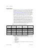
Table Of Contents
- SCXI-1121 User Manual
- Support
- Important Information
- Contents
- About This Manual
- Chapter 1 Introduction
- Chapter 2 Configuration and Installation
- Chapter 3 Theory of Operation
- Chapter 4 Register Descriptions
- Chapter 5 Programming
- Appendix A Specifications
- Appendix B Rear Signal Connector
- Appendix C SCXIbus Connector
- Appendix D SCXI-1121 Front Connector
- Appendix E SCXI-1121 Cabling
- Appendix F Revision A and B Photo and Parts Locator Diagrams
- Appendix G Technical Support Resources
- Glossary
- Index
- Figures
- Figure 2-1. SCXI-1121 General Parts Locator Diagram
- Figure 2-2. SCXI-1121 Detailed Parts Locator Diagram
- Figure 2-3. SCXI-1121 Front Connector Pin Assignment
- Figure 2-4. Ground-Referenced Signal Connection with High Common-Mode Voltage
- Figure 2-5. Floating Signal Connection Referenced to Chassis Ground for Better Signal-to-Noise Ratio
- Figure 2-6. Floating AC-Coupled Signal Connection
- Figure 2-7. AC-Coupled Signal Connection with High Common-Mode Voltage
- Figure 2-8. Assembling and Mounting the SCXI-1330 Connector-and-Shell Assembly
- Figure 2-9. Nulling Circuit
- Figure 2-10. Shunt Circuit
- Figure 2-11. SCXI-1320 Parts Locator Diagram
- Figure 2-12. SCXI-1328 Parts Locator Diagram
- Figure 2-13. SCXI-1321 Parts Locator Diagram
- Figure 2-14. SCXI-1121 Rear Signal Connector Pin Assignment
- Figure 2-15. SCANCLK Timing Requirements
- Figure 2-16. Slot-Select Timing Diagram
- Figure 2-17. Serial Data Timing Diagram
- Figure 2-18. Configuration Register Write Timing Diagram
- Figure 2-19. SCXI-1121 Module ID Register Timing Diagram
- Figure 3-1. SCXI-1121 Block Diagram
- Figure 3-2. SCXIbus Connector Pin Assignment
- Figure 3-3. Digital Interface Circuitry Block Diagram
- Figure 3-4. SCXI-1121 Digital Control
- Figure 3-5. Analog Input Block Diagram
- Figure 3-6. Analog Output Circuitry
- Figure 3-7. Single-Module Parallel Scanning
- Figure 3-8. Single-Module Multiplexed Scanning (Direct)
- Figure 3-9. Single-Module Multiplexed Scanning (Indirect)
- Figure 3-10. Multiple-Module Multiplexed Scanning
- Figure 3-11. Multiple-Chassis Scanning
- Figure B-1. SCXI-1121 Rear Signal Connector Pin Assignment
- Figure C-1. SCXIbus Connector Pin Assignment
- Figure D-1. SCXI-1121 Front Connector Pin Assignment
- Figure E-1. SCXI-1340 Installation
- Figure E-2. SCXI-1180 Rear Connections
- Figure E-3. SCXI-1180 Front Panel Installation
- Figure E-4. Cover Removal
- Figure F-1. Revision A and B SCXI-1121 Signal Conditioning Module
- Figure F-2. Revision A and B SCXI-1121 General Parts Locator Diagram
- Figure F-3. Revision A and B SCXI-1121 Detailed Parts Locator Diagram
- Tables
- Table 2-1. Digital Signal Connections, Jumper Settings
- Table 2-2. Jumper W33 Settings
- Table 2-3. Gain Jumper Allocation
- Table 2-4. Gain Jumper Positions
- Table 2-5. Filter Jumper Allocation
- Table 2-6. Voltage and Current Mode Excitation Jumper Setup
- Table 2-7. Maximum Load per Excitation Channel
- Table 2-8. Excitation Level Jumper Selection
- Table 2-9. Completion Network Jumpers
- Table 2-10. Trimmer Potentiometer and Corresponding Channel
- Table 2-11. Nulling Resistors and Corresponding Channel
- Table 2-12. Jumper Settings of the Nulling Circuits
- Table 2-13. Jumper Settings on the SCXI-1320 Terminal Block
- Table 2-14. Jumper Settings on the SCXI-1328 Terminal Block
- Table 2-15. Jumper Settings on the SCXI-1321 Terminal Block
- Table 2-16. SCXIbus to SCXI-1121 Rear Signal Connector to Data Acquisition Board Pin Equivalences
- Table 3-1. SCXIbus Equivalents for the Rear Signal Connector
- Table 3-2. Calibration Potentiometer Reference Designators
- Table 5-1. SCXI-1121 Rear Signal Connector Pin Equivalences
- Table E-1. SCXI-1121 and MIO-16 Pinout Equivalences
- Table E-2. SCXI-1341 and SCXI-1344 Pin Translations
- Table E-3. SCXI-1342 Pin Translations
- Table E-4. SCXI-1343 Pin Connections

Chapter 4 Register Descriptions
© National Instruments Corporation 4-9 SCXI-1121 User Manual
FIFO Register
The FIFO Register is used to add entries to the Slot 0 FIFO. The FIFO contains the Slot 0 scan
list. Each entry contains a slot number to be accessed, and a count number to determine the
number of samples to be taken from that slot. To write to the FIFO Register, follow the
procedure given in the Register Writes section of Chapter 5, Programming, using 14 as the
slot number, and writing 16 bits to the FIFO Register. The register will shift in the data present
on the MOSI line, bit 15 first, when Slot 14 is selected by the Slot-Select Register. The Slot 0
scan list is created by consecutive writes to the FIFO Register. Each write creates a new entry
at the end of the scan list. The maximum number of entries is 256. To clear the FIFO of all
entries, clear the HSRS* bit in the HSCR.
Type: Write-only
Word Size: 16-bit
Bit Map:
Bit Name Description
15-11 X Don’t care bits—Unused.
10-7 MOD<3..0>Module Number—The value of these bits plus
on determines the number of the slot to be accessed for this
scan entry. For example, to access Slot 6, MOD<3..0>
would be 0101.
6-0 CNT<6..0> Count—The value of these bits plus one determines how
many samples will be taken before the next scan list entry
becomes active. A value of zero corresponds to one sample
and a value of 127 corresponds to 128 samples.
15 14 13 12 11 10 9 8
X X X X X MOD3 MOD2 MOD1
76543210
MOD0 CNT6 CNT5 CNT4 CNT3 CNT2 CNT1 CNT0