
Network Card User Manual
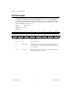
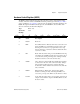
Table Of Contents
- SCXI-1121 User Manual
- Support
- Important Information
- Contents
- About This Manual
- Chapter 1 Introduction
- Chapter 2 Configuration and Installation
- Chapter 3 Theory of Operation
- Chapter 4 Register Descriptions
- Chapter 5 Programming
- Appendix A Specifications
- Appendix B Rear Signal Connector
- Appendix C SCXIbus Connector
- Appendix D SCXI-1121 Front Connector
- Appendix E SCXI-1121 Cabling
- Appendix F Revision A and B Photo and Parts Locator Diagrams
- Appendix G Technical Support Resources
- Glossary
- Index
- Figures
- Figure 2-1. SCXI-1121 General Parts Locator Diagram
- Figure 2-2. SCXI-1121 Detailed Parts Locator Diagram
- Figure 2-3. SCXI-1121 Front Connector Pin Assignment
- Figure 2-4. Ground-Referenced Signal Connection with High Common-Mode Voltage
- Figure 2-5. Floating Signal Connection Referenced to Chassis Ground for Better Signal-to-Noise Ratio
- Figure 2-6. Floating AC-Coupled Signal Connection
- Figure 2-7. AC-Coupled Signal Connection with High Common-Mode Voltage
- Figure 2-8. Assembling and Mounting the SCXI-1330 Connector-and-Shell Assembly
- Figure 2-9. Nulling Circuit
- Figure 2-10. Shunt Circuit
- Figure 2-11. SCXI-1320 Parts Locator Diagram
- Figure 2-12. SCXI-1328 Parts Locator Diagram
- Figure 2-13. SCXI-1321 Parts Locator Diagram
- Figure 2-14. SCXI-1121 Rear Signal Connector Pin Assignment
- Figure 2-15. SCANCLK Timing Requirements
- Figure 2-16. Slot-Select Timing Diagram
- Figure 2-17. Serial Data Timing Diagram
- Figure 2-18. Configuration Register Write Timing Diagram
- Figure 2-19. SCXI-1121 Module ID Register Timing Diagram
- Figure 3-1. SCXI-1121 Block Diagram
- Figure 3-2. SCXIbus Connector Pin Assignment
- Figure 3-3. Digital Interface Circuitry Block Diagram
- Figure 3-4. SCXI-1121 Digital Control
- Figure 3-5. Analog Input Block Diagram
- Figure 3-6. Analog Output Circuitry
- Figure 3-7. Single-Module Parallel Scanning
- Figure 3-8. Single-Module Multiplexed Scanning (Direct)
- Figure 3-9. Single-Module Multiplexed Scanning (Indirect)
- Figure 3-10. Multiple-Module Multiplexed Scanning
- Figure 3-11. Multiple-Chassis Scanning
- Figure B-1. SCXI-1121 Rear Signal Connector Pin Assignment
- Figure C-1. SCXIbus Connector Pin Assignment
- Figure D-1. SCXI-1121 Front Connector Pin Assignment
- Figure E-1. SCXI-1340 Installation
- Figure E-2. SCXI-1180 Rear Connections
- Figure E-3. SCXI-1180 Front Panel Installation
- Figure E-4. Cover Removal
- Figure F-1. Revision A and B SCXI-1121 Signal Conditioning Module
- Figure F-2. Revision A and B SCXI-1121 General Parts Locator Diagram
- Figure F-3. Revision A and B SCXI-1121 Detailed Parts Locator Diagram
- Tables
- Table 2-1. Digital Signal Connections, Jumper Settings
- Table 2-2. Jumper W33 Settings
- Table 2-3. Gain Jumper Allocation
- Table 2-4. Gain Jumper Positions
- Table 2-5. Filter Jumper Allocation
- Table 2-6. Voltage and Current Mode Excitation Jumper Setup
- Table 2-7. Maximum Load per Excitation Channel
- Table 2-8. Excitation Level Jumper Selection
- Table 2-9. Completion Network Jumpers
- Table 2-10. Trimmer Potentiometer and Corresponding Channel
- Table 2-11. Nulling Resistors and Corresponding Channel
- Table 2-12. Jumper Settings of the Nulling Circuits
- Table 2-13. Jumper Settings on the SCXI-1320 Terminal Block
- Table 2-14. Jumper Settings on the SCXI-1328 Terminal Block
- Table 2-15. Jumper Settings on the SCXI-1321 Terminal Block
- Table 2-16. SCXIbus to SCXI-1121 Rear Signal Connector to Data Acquisition Board Pin Equivalences
- Table 3-1. SCXIbus Equivalents for the Rear Signal Connector
- Table 3-2. Calibration Potentiometer Reference Designators
- Table 5-1. SCXI-1121 Rear Signal Connector Pin Equivalences
- Table E-1. SCXI-1121 and MIO-16 Pinout Equivalences
- Table E-2. SCXI-1341 and SCXI-1344 Pin Translations
- Table E-3. SCXI-1342 Pin Translations
- Table E-4. SCXI-1343 Pin Connections

Chapter 4 Register Descriptions
© National Instruments Corporation 4-7 SCXI-1121 User Manual
Hardscan Control Register (HSCR)
The HSCR contains eight bits that control the setup and operation of the hardscan timing
circuitry of Slot 0. To write to the HSCR, follow the procedure given in the Register Writes
section of Chapter 5, Programming, using 13 as the slot number, and writing eight bits to the
HSCR. The register will shift in the data present on the MOSI line, bit seven first, when
Slot 13 is selected by the Slot-Select Register.
Type: Write-only
Word Size: 8-bit
Bit Map:
Bit Name Description
7 RSVD Reserved.
6 FRT Forced Retransmit—This bit, when clear, causes the scan
list in the FIFO to be reinitialized to the first entry, thus
allowing the scan list to be reprogrammed in two steps
instead of having to rewrite the entire list. When this bit is
set, it has no effect.
5 RD Read—This bit, when clear, prevents the FIFO from being
read. When set, the FIFO is being read except at the end of
a scan list entry during scanning, when reading is briefly
disabled to advance to the next scan list entry.
4 ONCE Once—When set, this bit will cause the Hardscan circuitry
to shut down at the end of the scan list circuitry during a
data acquisition. When clear, the circuitry will wrap
around and continue with the first scan list entry after the
entry is finished.
3 HSRS* Hardscan Reset—When clear, this bit causes all the
hardware scanning circuitry, including the FIFO, to be
reset to the power up state. When set, this bit has no effect.
2 LOAD* Load—This bit, when clear, forces a loading of the Slot 0
sample counter with the output of the FIFO. When set, this
bit has no effect.
765432 1 0
RSVD FRT RD ONCE HSRS* LOAD* SCANCONEN CLKEN