
Network Card User Manual
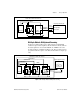
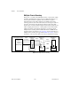
Table Of Contents
- SCXI-1121 User Manual
- Support
- Important Information
- Contents
- About This Manual
- Chapter 1 Introduction
- Chapter 2 Configuration and Installation
- Chapter 3 Theory of Operation
- Chapter 4 Register Descriptions
- Chapter 5 Programming
- Appendix A Specifications
- Appendix B Rear Signal Connector
- Appendix C SCXIbus Connector
- Appendix D SCXI-1121 Front Connector
- Appendix E SCXI-1121 Cabling
- Appendix F Revision A and B Photo and Parts Locator Diagrams
- Appendix G Technical Support Resources
- Glossary
- Index
- Figures
- Figure 2-1. SCXI-1121 General Parts Locator Diagram
- Figure 2-2. SCXI-1121 Detailed Parts Locator Diagram
- Figure 2-3. SCXI-1121 Front Connector Pin Assignment
- Figure 2-4. Ground-Referenced Signal Connection with High Common-Mode Voltage
- Figure 2-5. Floating Signal Connection Referenced to Chassis Ground for Better Signal-to-Noise Ratio
- Figure 2-6. Floating AC-Coupled Signal Connection
- Figure 2-7. AC-Coupled Signal Connection with High Common-Mode Voltage
- Figure 2-8. Assembling and Mounting the SCXI-1330 Connector-and-Shell Assembly
- Figure 2-9. Nulling Circuit
- Figure 2-10. Shunt Circuit
- Figure 2-11. SCXI-1320 Parts Locator Diagram
- Figure 2-12. SCXI-1328 Parts Locator Diagram
- Figure 2-13. SCXI-1321 Parts Locator Diagram
- Figure 2-14. SCXI-1121 Rear Signal Connector Pin Assignment
- Figure 2-15. SCANCLK Timing Requirements
- Figure 2-16. Slot-Select Timing Diagram
- Figure 2-17. Serial Data Timing Diagram
- Figure 2-18. Configuration Register Write Timing Diagram
- Figure 2-19. SCXI-1121 Module ID Register Timing Diagram
- Figure 3-1. SCXI-1121 Block Diagram
- Figure 3-2. SCXIbus Connector Pin Assignment
- Figure 3-3. Digital Interface Circuitry Block Diagram
- Figure 3-4. SCXI-1121 Digital Control
- Figure 3-5. Analog Input Block Diagram
- Figure 3-6. Analog Output Circuitry
- Figure 3-7. Single-Module Parallel Scanning
- Figure 3-8. Single-Module Multiplexed Scanning (Direct)
- Figure 3-9. Single-Module Multiplexed Scanning (Indirect)
- Figure 3-10. Multiple-Module Multiplexed Scanning
- Figure 3-11. Multiple-Chassis Scanning
- Figure B-1. SCXI-1121 Rear Signal Connector Pin Assignment
- Figure C-1. SCXIbus Connector Pin Assignment
- Figure D-1. SCXI-1121 Front Connector Pin Assignment
- Figure E-1. SCXI-1340 Installation
- Figure E-2. SCXI-1180 Rear Connections
- Figure E-3. SCXI-1180 Front Panel Installation
- Figure E-4. Cover Removal
- Figure F-1. Revision A and B SCXI-1121 Signal Conditioning Module
- Figure F-2. Revision A and B SCXI-1121 General Parts Locator Diagram
- Figure F-3. Revision A and B SCXI-1121 Detailed Parts Locator Diagram
- Tables
- Table 2-1. Digital Signal Connections, Jumper Settings
- Table 2-2. Jumper W33 Settings
- Table 2-3. Gain Jumper Allocation
- Table 2-4. Gain Jumper Positions
- Table 2-5. Filter Jumper Allocation
- Table 2-6. Voltage and Current Mode Excitation Jumper Setup
- Table 2-7. Maximum Load per Excitation Channel
- Table 2-8. Excitation Level Jumper Selection
- Table 2-9. Completion Network Jumpers
- Table 2-10. Trimmer Potentiometer and Corresponding Channel
- Table 2-11. Nulling Resistors and Corresponding Channel
- Table 2-12. Jumper Settings of the Nulling Circuits
- Table 2-13. Jumper Settings on the SCXI-1320 Terminal Block
- Table 2-14. Jumper Settings on the SCXI-1328 Terminal Block
- Table 2-15. Jumper Settings on the SCXI-1321 Terminal Block
- Table 2-16. SCXIbus to SCXI-1121 Rear Signal Connector to Data Acquisition Board Pin Equivalences
- Table 3-1. SCXIbus Equivalents for the Rear Signal Connector
- Table 3-2. Calibration Potentiometer Reference Designators
- Table 5-1. SCXI-1121 Rear Signal Connector Pin Equivalences
- Table E-1. SCXI-1121 and MIO-16 Pinout Equivalences
- Table E-2. SCXI-1341 and SCXI-1344 Pin Translations
- Table E-3. SCXI-1342 Pin Translations
- Table E-4. SCXI-1343 Pin Connections
Chapter 4 Register Descriptions
© National Instruments Corporation 4-5 SCXI-1121 User Manual
0 FOUTEN* Forced Output Enable—This bit determines whether the
module will drive the MCH0± pins on the rear signal
connector with either the selected channel output or the
MTEMP signal, depending on the state of RTEMP. If
FOUTEN* is cleared to zero, the MCH0± pins will be
driven through a buffer by the selected channel output or
the MTEMP line. If FOUTEN* is set to one, the MCH0±
pins will not be driven by the selected channel output or
MTEMP, unless SCANCON is active (low) and the
SCANCONEN bit is cleared. If the selected channel
output or MTEMP is driving the output buffer, it will drive
Analog Bus 0 if AB0EN is set. If nothing is driving the
output buffer, the SCXI-1121 output will saturate.
Slot 0 Register Descriptions
Slot 0 has three registers. The Slot-Select Register is a 16-bit, write-only
register that determines with which slot the data acquisition board will
speak when SLOT0SEL* is released high. In the case of the SCXI-1001
chassis, the Slot-Select Register also determines in which chassis the
desired slot is. The FIFO Register is a 16-bit, write-only register used for
storing the Slot 0 scan list that determines the chassis scan sequence. The
Hardscan Control Register (HSCR) is an 8-bit, write-only register used for
setting up the timing circuitry in Slot 0. The Slot-Select Register is written
to by using the SLOT0SEL* line. The HSCR and the FIFO Register are
written to as if they were registers located on modules in Slots 13 and 14.
It is recommended that you maintain software copies of the Slot-Select
Register, HSCRs, and all the Slot 0 scan lists that correspond to the writes
to FIFO Registers.
If you are using multiple chassis, it is important to understand the
architectural differences of the Slot-Select Register as compared to the
HSCR and the FIFO Register. Although each chassis has its own physical
Slot-Select Register, all are written to at the same time. The jumper settings
in Slot 0 of a chassis determine with which chassis number Slot 0 is
identified. From the software perspective, only one Slot-Select Register
exists in a system composed of multiple chassis. The HSCR and FIFO
Register, on the other hand, are unique to each chassis and you must
program them separately.