
Network Card User Manual
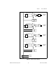
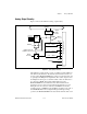
Table Of Contents
- SCXI-1121 User Manual
- Support
- Important Information
- Contents
- About This Manual
- Chapter 1 Introduction
- Chapter 2 Configuration and Installation
- Chapter 3 Theory of Operation
- Chapter 4 Register Descriptions
- Chapter 5 Programming
- Appendix A Specifications
- Appendix B Rear Signal Connector
- Appendix C SCXIbus Connector
- Appendix D SCXI-1121 Front Connector
- Appendix E SCXI-1121 Cabling
- Appendix F Revision A and B Photo and Parts Locator Diagrams
- Appendix G Technical Support Resources
- Glossary
- Index
- Figures
- Figure 2-1. SCXI-1121 General Parts Locator Diagram
- Figure 2-2. SCXI-1121 Detailed Parts Locator Diagram
- Figure 2-3. SCXI-1121 Front Connector Pin Assignment
- Figure 2-4. Ground-Referenced Signal Connection with High Common-Mode Voltage
- Figure 2-5. Floating Signal Connection Referenced to Chassis Ground for Better Signal-to-Noise Ratio
- Figure 2-6. Floating AC-Coupled Signal Connection
- Figure 2-7. AC-Coupled Signal Connection with High Common-Mode Voltage
- Figure 2-8. Assembling and Mounting the SCXI-1330 Connector-and-Shell Assembly
- Figure 2-9. Nulling Circuit
- Figure 2-10. Shunt Circuit
- Figure 2-11. SCXI-1320 Parts Locator Diagram
- Figure 2-12. SCXI-1328 Parts Locator Diagram
- Figure 2-13. SCXI-1321 Parts Locator Diagram
- Figure 2-14. SCXI-1121 Rear Signal Connector Pin Assignment
- Figure 2-15. SCANCLK Timing Requirements
- Figure 2-16. Slot-Select Timing Diagram
- Figure 2-17. Serial Data Timing Diagram
- Figure 2-18. Configuration Register Write Timing Diagram
- Figure 2-19. SCXI-1121 Module ID Register Timing Diagram
- Figure 3-1. SCXI-1121 Block Diagram
- Figure 3-2. SCXIbus Connector Pin Assignment
- Figure 3-3. Digital Interface Circuitry Block Diagram
- Figure 3-4. SCXI-1121 Digital Control
- Figure 3-5. Analog Input Block Diagram
- Figure 3-6. Analog Output Circuitry
- Figure 3-7. Single-Module Parallel Scanning
- Figure 3-8. Single-Module Multiplexed Scanning (Direct)
- Figure 3-9. Single-Module Multiplexed Scanning (Indirect)
- Figure 3-10. Multiple-Module Multiplexed Scanning
- Figure 3-11. Multiple-Chassis Scanning
- Figure B-1. SCXI-1121 Rear Signal Connector Pin Assignment
- Figure C-1. SCXIbus Connector Pin Assignment
- Figure D-1. SCXI-1121 Front Connector Pin Assignment
- Figure E-1. SCXI-1340 Installation
- Figure E-2. SCXI-1180 Rear Connections
- Figure E-3. SCXI-1180 Front Panel Installation
- Figure E-4. Cover Removal
- Figure F-1. Revision A and B SCXI-1121 Signal Conditioning Module
- Figure F-2. Revision A and B SCXI-1121 General Parts Locator Diagram
- Figure F-3. Revision A and B SCXI-1121 Detailed Parts Locator Diagram
- Tables
- Table 2-1. Digital Signal Connections, Jumper Settings
- Table 2-2. Jumper W33 Settings
- Table 2-3. Gain Jumper Allocation
- Table 2-4. Gain Jumper Positions
- Table 2-5. Filter Jumper Allocation
- Table 2-6. Voltage and Current Mode Excitation Jumper Setup
- Table 2-7. Maximum Load per Excitation Channel
- Table 2-8. Excitation Level Jumper Selection
- Table 2-9. Completion Network Jumpers
- Table 2-10. Trimmer Potentiometer and Corresponding Channel
- Table 2-11. Nulling Resistors and Corresponding Channel
- Table 2-12. Jumper Settings of the Nulling Circuits
- Table 2-13. Jumper Settings on the SCXI-1320 Terminal Block
- Table 2-14. Jumper Settings on the SCXI-1328 Terminal Block
- Table 2-15. Jumper Settings on the SCXI-1321 Terminal Block
- Table 2-16. SCXIbus to SCXI-1121 Rear Signal Connector to Data Acquisition Board Pin Equivalences
- Table 3-1. SCXIbus Equivalents for the Rear Signal Connector
- Table 3-2. Calibration Potentiometer Reference Designators
- Table 5-1. SCXI-1121 Rear Signal Connector Pin Equivalences
- Table E-1. SCXI-1121 and MIO-16 Pinout Equivalences
- Table E-2. SCXI-1341 and SCXI-1344 Pin Translations
- Table E-3. SCXI-1342 Pin Translations
- Table E-4. SCXI-1343 Pin Connections
Chapter 3 Theory of Operation
© National Instruments Corporation 3-17 SCXI-1121 User Manual
Scanning Modes
There are four basic types of scanning modes possible with the
SCXI-1121—single-module parallel scanning, single-module multiplexed
scanning, multiple-module multiplexed scanning, and multiple-chassis
scanning (possible only with the SCXI-1001 chassis). For additional
information, consult Chapter 2, Configuration and Installation, Chapter 5,
Programming, your data acquisition board manual, and your SCXI chassis
user manual. If you need further information, contact National Instruments.
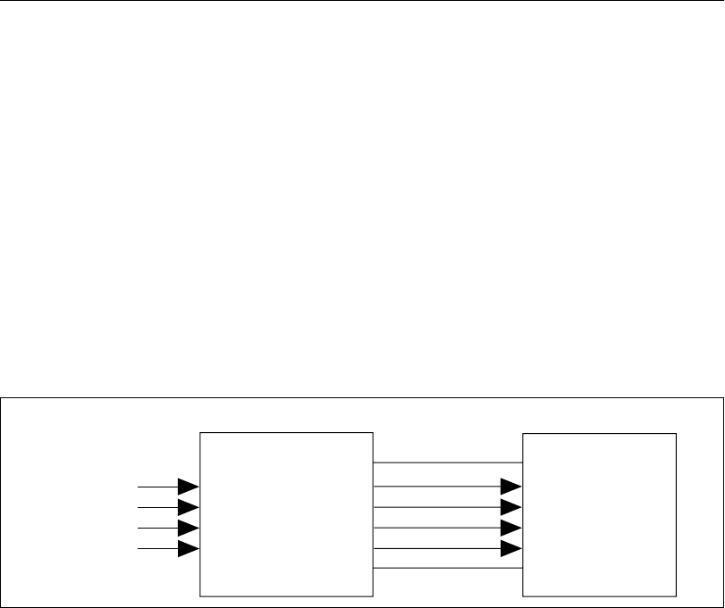
Single-Module Parallel Scanning
Single-Module parallel scanning is the simplest scanning mode. Directly
cable the SCXI-1121 to the data acquisition board as shown in Figure 3-7.
In this configuration, each analog signal has its own channel. Timing
signals are not necessary for this type of scanning because the module
provides all channels to the data acquisition board at all times. You can
implement single-module parallel scanning with any data acquisition board
that is appropriately cabled to the SCXI-1121.
Figure 3-7.
Single-Module Parallel Scanning
Multiplexed Scanning
Only the MIO-16 data acquisition boards support multiplexed scanning on
the SCXI-1121. During multiplexed scanning, a module sends the
SCANCLK signal to Slot 0 over the TRIG0 backplane line, and Slot 0
sends unique SCANCON signals to each module. Each module uses its
signal to reload MUXCOUNTER and to determine when the SCXI-1121
output is enabled. Slot 0 contains a module list first-in-first-out (FIFO)
memory chip, similar to the Channel/Gain FIFO on an MIO-16 board,
except that instead of having a channel number and gain setting for each
entry, the Slot 0 FIFO contains a slot number and a sample count for each
Four Isolated
Floating
Single-Ended
Inputs
CH0
CH1
CH2
CH3
MCH0
MCH1
MCH2
MCH3
Analog Input 0
Analog Input 1
Analog Input 2
Analog Input 3
Data Acquisition BoardSCXI-1121
Cable Assembly