
Network Card User Manual
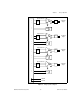
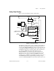
Table Of Contents
- SCXI-1121 User Manual
- Support
- Important Information
- Contents
- About This Manual
- Chapter 1 Introduction
- Chapter 2 Configuration and Installation
- Chapter 3 Theory of Operation
- Chapter 4 Register Descriptions
- Chapter 5 Programming
- Appendix A Specifications
- Appendix B Rear Signal Connector
- Appendix C SCXIbus Connector
- Appendix D SCXI-1121 Front Connector
- Appendix E SCXI-1121 Cabling
- Appendix F Revision A and B Photo and Parts Locator Diagrams
- Appendix G Technical Support Resources
- Glossary
- Index
- Figures
- Figure 2-1. SCXI-1121 General Parts Locator Diagram
- Figure 2-2. SCXI-1121 Detailed Parts Locator Diagram
- Figure 2-3. SCXI-1121 Front Connector Pin Assignment
- Figure 2-4. Ground-Referenced Signal Connection with High Common-Mode Voltage
- Figure 2-5. Floating Signal Connection Referenced to Chassis Ground for Better Signal-to-Noise Ratio
- Figure 2-6. Floating AC-Coupled Signal Connection
- Figure 2-7. AC-Coupled Signal Connection with High Common-Mode Voltage
- Figure 2-8. Assembling and Mounting the SCXI-1330 Connector-and-Shell Assembly
- Figure 2-9. Nulling Circuit
- Figure 2-10. Shunt Circuit
- Figure 2-11. SCXI-1320 Parts Locator Diagram
- Figure 2-12. SCXI-1328 Parts Locator Diagram
- Figure 2-13. SCXI-1321 Parts Locator Diagram
- Figure 2-14. SCXI-1121 Rear Signal Connector Pin Assignment
- Figure 2-15. SCANCLK Timing Requirements
- Figure 2-16. Slot-Select Timing Diagram
- Figure 2-17. Serial Data Timing Diagram
- Figure 2-18. Configuration Register Write Timing Diagram
- Figure 2-19. SCXI-1121 Module ID Register Timing Diagram
- Figure 3-1. SCXI-1121 Block Diagram
- Figure 3-2. SCXIbus Connector Pin Assignment
- Figure 3-3. Digital Interface Circuitry Block Diagram
- Figure 3-4. SCXI-1121 Digital Control
- Figure 3-5. Analog Input Block Diagram
- Figure 3-6. Analog Output Circuitry
- Figure 3-7. Single-Module Parallel Scanning
- Figure 3-8. Single-Module Multiplexed Scanning (Direct)
- Figure 3-9. Single-Module Multiplexed Scanning (Indirect)
- Figure 3-10. Multiple-Module Multiplexed Scanning
- Figure 3-11. Multiple-Chassis Scanning
- Figure B-1. SCXI-1121 Rear Signal Connector Pin Assignment
- Figure C-1. SCXIbus Connector Pin Assignment
- Figure D-1. SCXI-1121 Front Connector Pin Assignment
- Figure E-1. SCXI-1340 Installation
- Figure E-2. SCXI-1180 Rear Connections
- Figure E-3. SCXI-1180 Front Panel Installation
- Figure E-4. Cover Removal
- Figure F-1. Revision A and B SCXI-1121 Signal Conditioning Module
- Figure F-2. Revision A and B SCXI-1121 General Parts Locator Diagram
- Figure F-3. Revision A and B SCXI-1121 Detailed Parts Locator Diagram
- Tables
- Table 2-1. Digital Signal Connections, Jumper Settings
- Table 2-2. Jumper W33 Settings
- Table 2-3. Gain Jumper Allocation
- Table 2-4. Gain Jumper Positions
- Table 2-5. Filter Jumper Allocation
- Table 2-6. Voltage and Current Mode Excitation Jumper Setup
- Table 2-7. Maximum Load per Excitation Channel
- Table 2-8. Excitation Level Jumper Selection
- Table 2-9. Completion Network Jumpers
- Table 2-10. Trimmer Potentiometer and Corresponding Channel
- Table 2-11. Nulling Resistors and Corresponding Channel
- Table 2-12. Jumper Settings of the Nulling Circuits
- Table 2-13. Jumper Settings on the SCXI-1320 Terminal Block
- Table 2-14. Jumper Settings on the SCXI-1328 Terminal Block
- Table 2-15. Jumper Settings on the SCXI-1321 Terminal Block
- Table 2-16. SCXIbus to SCXI-1121 Rear Signal Connector to Data Acquisition Board Pin Equivalences
- Table 3-1. SCXIbus Equivalents for the Rear Signal Connector
- Table 3-2. Calibration Potentiometer Reference Designators
- Table 5-1. SCXI-1121 Rear Signal Connector Pin Equivalences
- Table E-1. SCXI-1121 and MIO-16 Pinout Equivalences
- Table E-2. SCXI-1341 and SCXI-1344 Pin Translations
- Table E-3. SCXI-1342 Pin Translations
- Table E-4. SCXI-1343 Pin Connections
Chapter 3 Theory of Operation
SCXI-1121 User Manual 3-16 www.natinst.com
in the Configuration Register when SCANCON is high (inactive) and will
count upwards on each rising clock edge when SCANCON is low (active).
In the Parallel-Output Mode, the MUXCOUNTER is disabled and its
output indicates binary 00 hence, amplifier channel 0 is selected at the
output multiplexer and is connected to MCH0. The three other channels are
hardwired to MCH1 through MCH3 on the rear signal connector.
The output multiplexer multiplexes all four amplifier outputs and the
temperature sensor reading provided on the MTEMP line. To read the
temperature sensor when it is multiplexed with the other input channels, set
the RTEMP bit of the Configuration Register high. This measurement is
only software controlled. For hardware control of the temperature sensor
reading, connect the temperature sensor to MCH4+. Notice that MCH4–,
the DTS reference, is hardwired to the chassis ground. The multiplexer
output connects to the MCH0± and is connected to the data acquisition
board analog channel input. In the case of the MIO data acquisition boards,
MCH0± on the rear signal connector corresponds to ACH0 and ACH8.
Furthermore, you can bus the multiplexed output of the SCXI-1121 via
switches to AB0± on the SCXIbus and on to other modules. When you use
multiple modules, you can bus the output of the module via AB0 to the
module that is connected to the data acquisition board. In this case, the AB0
switches of all the modules are closed, whereas the output multiplexer of
all the modules but the one being read are disabled. Refer to Chapters 2
and 5 for further details on how to configure and program multiple
modules.
In addition to the Multiplexed-Output mode described in the previous
paragraph, you can operate the SCXI-1121 in Parallel-Output mode. In this
mode, you need no software—other than software used with your data
acquisition board—to control the scanning of the four channels or to
perform a single read. To access the temperature sensor in this mode,
configure the temperature sensor in the DTS mode. At power up or at reset,
amplifier channel 0 is selected on the output multiplexer, and hence
connects to MCH0. The other four channels (three amplifier channels and
one temperature channel) are hardwired to the rear signal connector. Notice
that even when you select the Multiplexed-Output mode, the SCXI-1121
drives the rear signal connector pins 5 through 12. The SCXI-1121 outputs
on the rear signal connector are short-circuit protected.
Refer to the following Scanning Modes section for further details on how
to scan the SCXI-1121 channels.