
Network Card User Manual
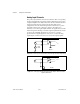
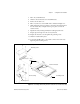
Table Of Contents
- SCXI-1121 User Manual
- Support
- Important Information
- Contents
- About This Manual
- Chapter 1 Introduction
- Chapter 2 Configuration and Installation
- Chapter 3 Theory of Operation
- Chapter 4 Register Descriptions
- Chapter 5 Programming
- Appendix A Specifications
- Appendix B Rear Signal Connector
- Appendix C SCXIbus Connector
- Appendix D SCXI-1121 Front Connector
- Appendix E SCXI-1121 Cabling
- Appendix F Revision A and B Photo and Parts Locator Diagrams
- Appendix G Technical Support Resources
- Glossary
- Index
- Figures
- Figure 2-1. SCXI-1121 General Parts Locator Diagram
- Figure 2-2. SCXI-1121 Detailed Parts Locator Diagram
- Figure 2-3. SCXI-1121 Front Connector Pin Assignment
- Figure 2-4. Ground-Referenced Signal Connection with High Common-Mode Voltage
- Figure 2-5. Floating Signal Connection Referenced to Chassis Ground for Better Signal-to-Noise Ratio
- Figure 2-6. Floating AC-Coupled Signal Connection
- Figure 2-7. AC-Coupled Signal Connection with High Common-Mode Voltage
- Figure 2-8. Assembling and Mounting the SCXI-1330 Connector-and-Shell Assembly
- Figure 2-9. Nulling Circuit
- Figure 2-10. Shunt Circuit
- Figure 2-11. SCXI-1320 Parts Locator Diagram
- Figure 2-12. SCXI-1328 Parts Locator Diagram
- Figure 2-13. SCXI-1321 Parts Locator Diagram
- Figure 2-14. SCXI-1121 Rear Signal Connector Pin Assignment
- Figure 2-15. SCANCLK Timing Requirements
- Figure 2-16. Slot-Select Timing Diagram
- Figure 2-17. Serial Data Timing Diagram
- Figure 2-18. Configuration Register Write Timing Diagram
- Figure 2-19. SCXI-1121 Module ID Register Timing Diagram
- Figure 3-1. SCXI-1121 Block Diagram
- Figure 3-2. SCXIbus Connector Pin Assignment
- Figure 3-3. Digital Interface Circuitry Block Diagram
- Figure 3-4. SCXI-1121 Digital Control
- Figure 3-5. Analog Input Block Diagram
- Figure 3-6. Analog Output Circuitry
- Figure 3-7. Single-Module Parallel Scanning
- Figure 3-8. Single-Module Multiplexed Scanning (Direct)
- Figure 3-9. Single-Module Multiplexed Scanning (Indirect)
- Figure 3-10. Multiple-Module Multiplexed Scanning
- Figure 3-11. Multiple-Chassis Scanning
- Figure B-1. SCXI-1121 Rear Signal Connector Pin Assignment
- Figure C-1. SCXIbus Connector Pin Assignment
- Figure D-1. SCXI-1121 Front Connector Pin Assignment
- Figure E-1. SCXI-1340 Installation
- Figure E-2. SCXI-1180 Rear Connections
- Figure E-3. SCXI-1180 Front Panel Installation
- Figure E-4. Cover Removal
- Figure F-1. Revision A and B SCXI-1121 Signal Conditioning Module
- Figure F-2. Revision A and B SCXI-1121 General Parts Locator Diagram
- Figure F-3. Revision A and B SCXI-1121 Detailed Parts Locator Diagram
- Tables
- Table 2-1. Digital Signal Connections, Jumper Settings
- Table 2-2. Jumper W33 Settings
- Table 2-3. Gain Jumper Allocation
- Table 2-4. Gain Jumper Positions
- Table 2-5. Filter Jumper Allocation
- Table 2-6. Voltage and Current Mode Excitation Jumper Setup
- Table 2-7. Maximum Load per Excitation Channel
- Table 2-8. Excitation Level Jumper Selection
- Table 2-9. Completion Network Jumpers
- Table 2-10. Trimmer Potentiometer and Corresponding Channel
- Table 2-11. Nulling Resistors and Corresponding Channel
- Table 2-12. Jumper Settings of the Nulling Circuits
- Table 2-13. Jumper Settings on the SCXI-1320 Terminal Block
- Table 2-14. Jumper Settings on the SCXI-1328 Terminal Block
- Table 2-15. Jumper Settings on the SCXI-1321 Terminal Block
- Table 2-16. SCXIbus to SCXI-1121 Rear Signal Connector to Data Acquisition Board Pin Equivalences
- Table 3-1. SCXIbus Equivalents for the Rear Signal Connector
- Table 3-2. Calibration Potentiometer Reference Designators
- Table 5-1. SCXI-1121 Rear Signal Connector Pin Equivalences
- Table E-1. SCXI-1121 and MIO-16 Pinout Equivalences
- Table E-2. SCXI-1341 and SCXI-1344 Pin Translations
- Table E-3. SCXI-1342 Pin Translations
- Table E-4. SCXI-1343 Pin Connections

Chapter 2 Configuration and Installation
SCXI-1121 User Manual 2-22 www.natinst.com
Warning Exceeding the input signal range and the common-mode input range results in
distorted signals. Exceeding the maximum input voltage rating (250 V
rms
between positive
and negative terminals and between any terminal and earth ground) can damage the
SCXI-1121, the SCXIbus, and the DAQ board. National Instruments is not liable for any
damages or injuries resulting from such signal connections.
Excitation Channels
Four fully isolated excitation channels are available. Each excitation
channel corresponds to an input channel. A 250 V
rms
isolation barrier exists
between two corresponding channels (for example, between input
channel 0 and excitation channel 0). In addition, the excitation outputs are
overvoltage protected to 250 V
rms
with current foldback.
Warning Exceeding the overvoltage protection or isolation rating on the excitation output
can damage the SCXI-1121, the SCXIbus, and the DAQ board. National Instruments is not
liable for any damages or injuries resulting from such signal connections.
Temperature Sensor Connection
Pins C2 and C4 are dedicated for connecting the temperature sensor to the
SCXI-1121. The temperature sensor is not isolated and is referenced to
chassis ground. The connection is overvoltage-protected to ±25 VDC with
power on and ±15 VDC with power off.
Warning Exceeding the overvoltage protection on the temperature connections can
damage the SCXI-1121, the SCXIbus, and the DAQ board. National Instruments is not
liable for any damages resulting from such signal connections.
Connector-and-Shell Assembly
Two types of signal connectors are available to connect the transducers to
the SCXI-1121 inputs. The first, the SCXI-1330 32-pin DIN C female
connector-and-shell assembly, is available in a kit listed in the Optional
Equipment section in Chapter 1, Introduction. The connector has eyelet
ends for easy hook-and-solder wire connection. With this kit, you can build
your own signal cable to connect to the SCXI-1121 inputs. After you have
built the cable, the shell covers and protects the connector. Perform the
following steps to assemble and mount the connector-and-shell assembly
to your SCXI module:
1. Refer to Figure 2-8, Assembling and Mounting the SCXI-1330
Connector-and-Shell Assembly, and the diagram included with your
SCXI-1330 kit to build the connector-and-shell assembly.
2. Turn off the computer that contains your DAQ board or disconnect the
board from your SCXI chassis.