
Network Card User Manual
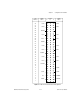
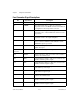
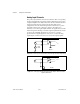
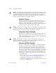
Table Of Contents
- SCXI-1121 User Manual
- Support
- Important Information
- Contents
- About This Manual
- Chapter 1 Introduction
- Chapter 2 Configuration and Installation
- Chapter 3 Theory of Operation
- Chapter 4 Register Descriptions
- Chapter 5 Programming
- Appendix A Specifications
- Appendix B Rear Signal Connector
- Appendix C SCXIbus Connector
- Appendix D SCXI-1121 Front Connector
- Appendix E SCXI-1121 Cabling
- Appendix F Revision A and B Photo and Parts Locator Diagrams
- Appendix G Technical Support Resources
- Glossary
- Index
- Figures
- Figure 2-1. SCXI-1121 General Parts Locator Diagram
- Figure 2-2. SCXI-1121 Detailed Parts Locator Diagram
- Figure 2-3. SCXI-1121 Front Connector Pin Assignment
- Figure 2-4. Ground-Referenced Signal Connection with High Common-Mode Voltage
- Figure 2-5. Floating Signal Connection Referenced to Chassis Ground for Better Signal-to-Noise Ratio
- Figure 2-6. Floating AC-Coupled Signal Connection
- Figure 2-7. AC-Coupled Signal Connection with High Common-Mode Voltage
- Figure 2-8. Assembling and Mounting the SCXI-1330 Connector-and-Shell Assembly
- Figure 2-9. Nulling Circuit
- Figure 2-10. Shunt Circuit
- Figure 2-11. SCXI-1320 Parts Locator Diagram
- Figure 2-12. SCXI-1328 Parts Locator Diagram
- Figure 2-13. SCXI-1321 Parts Locator Diagram
- Figure 2-14. SCXI-1121 Rear Signal Connector Pin Assignment
- Figure 2-15. SCANCLK Timing Requirements
- Figure 2-16. Slot-Select Timing Diagram
- Figure 2-17. Serial Data Timing Diagram
- Figure 2-18. Configuration Register Write Timing Diagram
- Figure 2-19. SCXI-1121 Module ID Register Timing Diagram
- Figure 3-1. SCXI-1121 Block Diagram
- Figure 3-2. SCXIbus Connector Pin Assignment
- Figure 3-3. Digital Interface Circuitry Block Diagram
- Figure 3-4. SCXI-1121 Digital Control
- Figure 3-5. Analog Input Block Diagram
- Figure 3-6. Analog Output Circuitry
- Figure 3-7. Single-Module Parallel Scanning
- Figure 3-8. Single-Module Multiplexed Scanning (Direct)
- Figure 3-9. Single-Module Multiplexed Scanning (Indirect)
- Figure 3-10. Multiple-Module Multiplexed Scanning
- Figure 3-11. Multiple-Chassis Scanning
- Figure B-1. SCXI-1121 Rear Signal Connector Pin Assignment
- Figure C-1. SCXIbus Connector Pin Assignment
- Figure D-1. SCXI-1121 Front Connector Pin Assignment
- Figure E-1. SCXI-1340 Installation
- Figure E-2. SCXI-1180 Rear Connections
- Figure E-3. SCXI-1180 Front Panel Installation
- Figure E-4. Cover Removal
- Figure F-1. Revision A and B SCXI-1121 Signal Conditioning Module
- Figure F-2. Revision A and B SCXI-1121 General Parts Locator Diagram
- Figure F-3. Revision A and B SCXI-1121 Detailed Parts Locator Diagram
- Tables
- Table 2-1. Digital Signal Connections, Jumper Settings
- Table 2-2. Jumper W33 Settings
- Table 2-3. Gain Jumper Allocation
- Table 2-4. Gain Jumper Positions
- Table 2-5. Filter Jumper Allocation
- Table 2-6. Voltage and Current Mode Excitation Jumper Setup
- Table 2-7. Maximum Load per Excitation Channel
- Table 2-8. Excitation Level Jumper Selection
- Table 2-9. Completion Network Jumpers
- Table 2-10. Trimmer Potentiometer and Corresponding Channel
- Table 2-11. Nulling Resistors and Corresponding Channel
- Table 2-12. Jumper Settings of the Nulling Circuits
- Table 2-13. Jumper Settings on the SCXI-1320 Terminal Block
- Table 2-14. Jumper Settings on the SCXI-1328 Terminal Block
- Table 2-15. Jumper Settings on the SCXI-1321 Terminal Block
- Table 2-16. SCXIbus to SCXI-1121 Rear Signal Connector to Data Acquisition Board Pin Equivalences
- Table 3-1. SCXIbus Equivalents for the Rear Signal Connector
- Table 3-2. Calibration Potentiometer Reference Designators
- Table 5-1. SCXI-1121 Rear Signal Connector Pin Equivalences
- Table E-1. SCXI-1121 and MIO-16 Pinout Equivalences
- Table E-2. SCXI-1341 and SCXI-1344 Pin Translations
- Table E-3. SCXI-1342 Pin Translations
- Table E-4. SCXI-1343 Pin Connections
Chapter 2 Configuration and Installation
SCXI-1121 User Manual 2-16 www.natinst.com
When connecting or disconnecting signal lines to the SCXI terminal block screw terminals,
make sure the lines are powered off. Potential differences between the lines and the SCXI
ground create a shock hazard while you connect the lines.
Connect the signal wires to the screw terminals by inserting the stripped end of the wire
fully into the terminals. Tighten the terminals to a torque of 5 to 7 in.-lb.
Connections, including power signals to ground and vice versa, that exceed any of the
maximum signal ratings on the SCXI device can create a shock or fire hazard or can
damage any or all of the boards connected to the SCXI chassis, the host computer, and the
SCXI device. National Instruments is not liable for any damages or injuries resulting from
incorrect signal connections.
If high voltages (≥30 Vrms and 42.4 V peak or 60 VDC) are present, you must connect a
safety earth ground wire to the terminal block safety ground solder lug. This complies with
safety agency requirements and protects against electric shock when the terminal block is
not connected to the chassis. To connect the safety earth ground to the safety ground solder
lug, run an earth ground wire in the cable from the signal source to the terminal block.
National Instruments is not liable for any damages or injuries resulting from inadequate
safety earth ground connections.
Do not loosen or re-orient the safety ground solder lug hardware when connecting the
safety ground wire. To do so reduces the safety isolation between the high voltage and
safety ground.
Clean devices and terminal blocks by brushing off light dust with a soft, nonmetallic brush.
Remove other contaminants with deionized water and a stiff nonmetallic brush. The unit
must be completely dry and free from contaminants before returning to service.
Use only National Instruments TBX Series cable assemblies with high-voltage TBX Series
terminal blocks.
Front Connector
Figure 2-3 shows the pin assignments for the SCXI-1121 front connector.