
Network Card User Manual
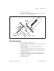
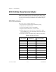
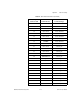
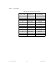
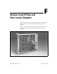
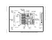
Table Of Contents
- SCXI-1121 User Manual
- Support
- Important Information
- Contents
- About This Manual
- Chapter 1 Introduction
- Chapter 2 Configuration and Installation
- Chapter 3 Theory of Operation
- Chapter 4 Register Descriptions
- Chapter 5 Programming
- Appendix A Specifications
- Appendix B Rear Signal Connector
- Appendix C SCXIbus Connector
- Appendix D SCXI-1121 Front Connector
- Appendix E SCXI-1121 Cabling
- Appendix F Revision A and B Photo and Parts Locator Diagrams
- Appendix G Technical Support Resources
- Glossary
- Index
- Figures
- Figure 2-1. SCXI-1121 General Parts Locator Diagram
- Figure 2-2. SCXI-1121 Detailed Parts Locator Diagram
- Figure 2-3. SCXI-1121 Front Connector Pin Assignment
- Figure 2-4. Ground-Referenced Signal Connection with High Common-Mode Voltage
- Figure 2-5. Floating Signal Connection Referenced to Chassis Ground for Better Signal-to-Noise Ratio
- Figure 2-6. Floating AC-Coupled Signal Connection
- Figure 2-7. AC-Coupled Signal Connection with High Common-Mode Voltage
- Figure 2-8. Assembling and Mounting the SCXI-1330 Connector-and-Shell Assembly
- Figure 2-9. Nulling Circuit
- Figure 2-10. Shunt Circuit
- Figure 2-11. SCXI-1320 Parts Locator Diagram
- Figure 2-12. SCXI-1328 Parts Locator Diagram
- Figure 2-13. SCXI-1321 Parts Locator Diagram
- Figure 2-14. SCXI-1121 Rear Signal Connector Pin Assignment
- Figure 2-15. SCANCLK Timing Requirements
- Figure 2-16. Slot-Select Timing Diagram
- Figure 2-17. Serial Data Timing Diagram
- Figure 2-18. Configuration Register Write Timing Diagram
- Figure 2-19. SCXI-1121 Module ID Register Timing Diagram
- Figure 3-1. SCXI-1121 Block Diagram
- Figure 3-2. SCXIbus Connector Pin Assignment
- Figure 3-3. Digital Interface Circuitry Block Diagram
- Figure 3-4. SCXI-1121 Digital Control
- Figure 3-5. Analog Input Block Diagram
- Figure 3-6. Analog Output Circuitry
- Figure 3-7. Single-Module Parallel Scanning
- Figure 3-8. Single-Module Multiplexed Scanning (Direct)
- Figure 3-9. Single-Module Multiplexed Scanning (Indirect)
- Figure 3-10. Multiple-Module Multiplexed Scanning
- Figure 3-11. Multiple-Chassis Scanning
- Figure B-1. SCXI-1121 Rear Signal Connector Pin Assignment
- Figure C-1. SCXIbus Connector Pin Assignment
- Figure D-1. SCXI-1121 Front Connector Pin Assignment
- Figure E-1. SCXI-1340 Installation
- Figure E-2. SCXI-1180 Rear Connections
- Figure E-3. SCXI-1180 Front Panel Installation
- Figure E-4. Cover Removal
- Figure F-1. Revision A and B SCXI-1121 Signal Conditioning Module
- Figure F-2. Revision A and B SCXI-1121 General Parts Locator Diagram
- Figure F-3. Revision A and B SCXI-1121 Detailed Parts Locator Diagram
- Tables
- Table 2-1. Digital Signal Connections, Jumper Settings
- Table 2-2. Jumper W33 Settings
- Table 2-3. Gain Jumper Allocation
- Table 2-4. Gain Jumper Positions
- Table 2-5. Filter Jumper Allocation
- Table 2-6. Voltage and Current Mode Excitation Jumper Setup
- Table 2-7. Maximum Load per Excitation Channel
- Table 2-8. Excitation Level Jumper Selection
- Table 2-9. Completion Network Jumpers
- Table 2-10. Trimmer Potentiometer and Corresponding Channel
- Table 2-11. Nulling Resistors and Corresponding Channel
- Table 2-12. Jumper Settings of the Nulling Circuits
- Table 2-13. Jumper Settings on the SCXI-1320 Terminal Block
- Table 2-14. Jumper Settings on the SCXI-1328 Terminal Block
- Table 2-15. Jumper Settings on the SCXI-1321 Terminal Block
- Table 2-16. SCXIbus to SCXI-1121 Rear Signal Connector to Data Acquisition Board Pin Equivalences
- Table 3-1. SCXIbus Equivalents for the Rear Signal Connector
- Table 3-2. Calibration Potentiometer Reference Designators
- Table 5-1. SCXI-1121 Rear Signal Connector Pin Equivalences
- Table E-1. SCXI-1121 and MIO-16 Pinout Equivalences
- Table E-2. SCXI-1341 and SCXI-1344 Pin Translations
- Table E-3. SCXI-1342 Pin Translations
- Table E-4. SCXI-1343 Pin Connections
Appendix E SCXI-1121 Cabling
© National Instruments Corporation E-13 SCXI-1121 User Manual
The adapter board has a male rear connector, a female front connector, and
a male chassis extender connector. You can attach the rear connector to a
ribbon cable from the MIO board or a preceding chassis. You connect the
front connector with the module rear signal connector. You connect the
chassis extender connector to a ribbon cable that goes to the subsequent
chassis. The adapter takes Channel 0 from the front connector and sends it
to Channel 0 of the rear connector. The adapter also takes channels 0
through 6 on the chassis extender connector and maps them to channels 1
through 7, respectively, on the rear connector.
SCXI-1350 Installation
Follow these steps to install the SCXI-1350:
1. Make sure that the computer and all the SCXI chassis are turned off.
2. Insert all the modules in all the chassis.
3. Connect one end of a ribbon cable to the MIO board.
4. Connect the other end of the ribbon cable to the rear connector of the
first SCXI-1350.
5. Connect another ribbon cable or cable assembly to the chassis extender
connector.
6. Plug the adapter board front connector to the module rear signal
connector. Make sure a corner of the adapter board enters the upper
board guide of the chassis.
7. Screw the rear panel to the threaded strips in the rear of the chassis.
8. Connect the cable assembly to the desired module in the second
chassis, or if you are using more than two chassis, connect the loose
end of the ribbon cable to the rear connector of the second SCXI-1350,
and install the adapter board.
9. Continue until all chassis are connected. For N chassis, you will need
N ribbon cables and N multichassis adapters.