Computer-Based Instruments NI 5401 User Manual PXI ™/PCI Arbitrary Function Generator NI 5401 User Manual March 1999 Edition Part Number 322419A-01
Worldwide Technical Support and Product Information www.natinst.
Important Information Warranty The NI 5401 is warranted against defects in materials and workmanship for a period of one year from the date of shipment, as evidenced by receipts or other documentation. National Instruments will, at its option, repair or replace equipment that proves to be defective during the warranty period. This warranty includes parts and labor.
Conventions The following conventions are used in this manual: » The » symbol leads you through nested menu items and dialog box options to a final action. The sequence File»Page Setup»Options directs you to pull down the File menu, select the Page Setup item, and select Options from the last dialog box. ♦ The ♦ symbol indicates that the following text applies only to a specific product, a specific operating system, or a specific software version.
Contents Chapter 1 Generating Functions with the NI 5401 About Your NI 5401 ......................................................................................................1-1 Connecting Signals ........................................................................................................1-2 ARB Connector ...............................................................................................1-3 SYNC Connector............................................................................
Contents SYNC Output and Duty Cycle........................................................................ 2-9 Output Attenuation.......................................................................................... 2-9 Output Impedance ........................................................................................... 2-10 Output Enable ................................................................................................. 2-10 Pre-Attenuation Offset ................................
Contents Figure 2-1. Figure 2-2. Figure 2-3. Figure 2-4. Figure 2-5. Figure 2-6. Figure 2-7. Figure 2-8. Figure 2-9. Figure 2-10. Figure 2-11. Figure 2-12. Figure 2-13. Figure 2-14. Figure 2-15. NI 5401 Block Diagram ........................................................................2-1 Waveform Data Path Block Diagram....................................................2-2 DDS Building Blocks............................................................................
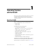
1 Generating Functions with the NI 5401 The NI 5401 User Manual describes the features, functions, and operation of the NI 5401 arbitrary function generator. This device performs comparably to standalone instruments while providing the flexibility of computer-based operation. About Your NI 5401 Thank you for buying a National Instruments NI 5401 arbitrary function generator.
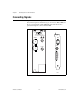
Chapter 1 Generating Functions with the NI 5401 Connecting Signals Figure 1-1 shows the front panels for the NI 5401 for the PXI and PCI buses. The front panel contains three types of connectors: BNC, SMB, and 50-pin very high-density SCSI (VHDSCSI). The main waveform is generated through the connector labeled ARB. LOCK ACCESS ARB OUT EXT TRIG PLL REF ARB SYNC PLL IN SYNC OUT PATTERN OUT PXI PCI Figure 1-1. NI 5401 I/O Connectors NI 5401 User Manual 1-2 www.natinst.
Chapter 1 Generating Functions with the NI 5401 ARB Connector The ARB connector provides the waveform output. The maximum output levels on this connector depend on the type of load termination. If the output of your NI 5401 terminates into a 50 Ω load, the output levels are ±5 V, as shown in Figure 1-2. If the output of your NI 5401 terminates into a high-impedance load (HiZ), the output levels are ±10 V.
Chapter 1 Generating Functions with the NI 5401 sine wave being generated and tw is the pulse width of the SYNC output. The duty cycle is (tw/tp) × 100%. tp ARB Output SYNC Output (50% Duty Cycle) tw SYNC Output (33% Duty Cycle) Figure 1-3. SYNC Output and Duty Cycle For your NI 5401 for PCI, you can route the SYNC output to the RTSI lines over the RTSI bus. For your NI 5401 for PXI, you can route the SYNC output to the TTL trigger lines over the TTL trigger bus.
Chapter 1 Generating Functions with the NI 5401 Pattern Out Connector (PCI Only) This connector is used on the NI 5401 for PCI to supply the external trigger input to the board. Connector Pin Assignments Figure 1-4 shows the NI 5401 50-pin digital connector. Refer to Table 1-1 for a description of the signals.
Chapter 1 Generating Functions with the NI 5401 Signal Descriptions Table 1-1 shows the pin names and signal descriptions used on the NI 5401 digital output connector. Table 1-1. Digital Connector Signal Descriptions Signal Name Type Description DGND – Digital ground EXT_TRIG Input External trigger—The external trigger input signal is a TTL-level signal that you can use to start or step through a waveform generation.
Chapter 1 Generating Functions with the NI 5401 RFU 1 35 DGND RFU 2 36 DGND RFU 3 37 DGND RFU 4 38 DGND RFU 5 39 DGND RFU 6 40 DGND RFU 7 41 DGND RFU 8 42 DGND RFU 9 43 DGND RFU 10 44 DGND RFU 11 45 DGND RFU 12 46 DGND RFU 13 47 DGND RFU 14 48 DGND RFU 15 49 DGND RFU 16 50 DGND RFU 17 51 DGND RFU 18 52 DGND RFU 19 53 DGND RFU 20 54 DGND RFU 21 55 DGND RFU 22 56 DGND RFU 23 57 DGND RFU 24 58 RFU NC 25 59 DGND
Chapter 1 Generating Functions with the NI 5401 Software Options for Your NI 5401 This section describes the NI-FGEN driver software and development tools that you can use to create application software for your NI 5401. Software Included with Your NI 5401 Your NI 5401 kit includes several VirtualBench soft front panels to help you get up and running quickly with your waveform generator. These soft front panels are an onscreen interface similar to standalone instruments.
Chapter 1 Generating Functions with the NI 5401 Waveform Editor You use the Waveform Editor to create, sketch, and edit complex waveforms that the VirtualBench-FG player can then generate. A library of standard waveforms for creating complex waveforms is included, and you can also write equations to create arbitrary waveforms and view the waveforms in a time or frequency domain.
Chapter 1 Generating Functions with the NI 5401 as C, including looping and case structures, configuration management tools, and compiled performance. Note Use the NI-FGEN instrument driver to program and control your NI 5401 using LabVIEW. LabWindows/CVI LabWindows/CVI is an interactive, ANSI C programming environment designed for automated test applications.
Chapter 1 Generating Functions with the NI 5401 Using the Soft Front Panels to Generate Waveforms You use the VirtualBench soft front panels to interactively control your NI 5401 as you would a desktop function generator. Generating Standard Functions If you need to generate standard waveforms such as a sine, square, ramp, or DC signal, you can use the VirtualBench-FG soft front panel shown in Figure 1-6. Launch the front panel by selecting Start»Programs»National Instruments FGEN»VirtualBench FG.
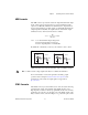
Chapter 1 Generating Functions with the NI 5401 To control additional instrument parameters, select Edit»54xx Settings to bring up the dialog box shown in Figures 1-7 and 1-8. Figure 1-7. VirtualBench-FG General Settings Dialog Box for the NI 5401 Figure 1-8. VirtualBench-FG Signals Settings Dialog Box for the NI 5401 Note Refer to the online help for further information about the 54xx Settings dialog box. NI 5401 User Manual 1-12 www.natinst.
Chapter 1 Generating Functions with the NI 5401 You can also load a custom waveform pattern with VirtualBench-FG. This waveform should be a text file and should contain exactly 16,384 samples. If the defined waveform does not contain exactly 16,384 samples, you may see undesired effects in your waveform output. Follow these steps to load a custom waveform: 1. Select File»Load Waveform to bring up the dialog box shown in Figure 1-9. Figure 1-9. VirtualBench-FG Load Waveform Dialog Box 2.
Chapter 1 Generating Functions with the NI 5401 them using the VirtualBench-FG Frequency List Editor. Follow these steps to create a list of multiple frequencies: 1. Select Window»Frequency List Editor from the VirtualBench-FG soft front panel to bring up the dialog box shown in Figure 1-10. Figure 1-10. VirtualBench-FG Frequency List Editor Dialog Box 2. Specify the frequency and duration of each function in the sequence. 3. Save the sequence by selecting File»Save. 4.
Chapter 1 Generating Functions with the NI 5401 Waveform Editor You can use the Waveform Editor shown in Figure 1-11 to create a custom waveform. To launch the Waveform Editor, select Start»Programs» National Instruments FGEN»Waveform Editor. You can select waveforms from the function library, write equations, or draw them manually. Each segment can have more than one waveform component in it, and you can perform a variety of math functions on each component. Figure 1-11.
Chapter 1 Generating Functions with the NI 5401 Power-Up and Reset Conditions When you power up your computer, the NI 5401 is in the following state: • The output is disabled and set to 0 V. • The trigger mode is set to continuous. • The trigger source is set to automatic (the software provides the triggers). • The digital filter is enabled. • Output attenuation remains unchanged from its previous setting. • The analog filter remains unchanged from its previous setting.
2 Function Generator Operation This chapter describes how to use your NI 5401. Figure 2-1 shows the NI 5401 block diagram. RTSI/PXI Trigger Bus DDS + Lookup Memory Instruction FIFOs Digital Filter IFIFO Control RTSI Control Clock Controls Waveform Sequencer DDS Control Filter Controls Trigger Control Analog Control DAC Attenuators, Filter, and Amplifier ARB SYNC Level Crossing Detector Data Path PLL Ref PLL and Clocking Bus Interface PXI/PCI Channel Figure 2-1.
Chapter 2 Function Generator Operation The NI 5401 has several main components: • A PXI or PCI bus interface that handles Plug and Play protocols for assigning resources to the device and providing drivers for the data and address bus that are local to the device • A waveform sequencer that performs multiple functions such as arbitrating the data buses and controlling the triggers, filters, attenuators, clocks, PLL, RTSI switch, instruction FIFO, and DDS • The data from the memory is fed to a digital
Chapter 2 Function Generator Operation Direct Digital Synthesis (DDS) Direct digital synthesis (DDS) is a technique for deriving, under digital control, an analog frequency source from a single reference clock frequency. This technique produces high-frequency accuracy and resolution, temperature stability, wideband tuning, and rapid and phase-continuous frequency switching. The NI 5401 uses a 32-bit, high-speed accumulator with a lookup memory and a 12-bit DAC for DDS-based waveform generation.
Chapter 2 Function Generator Operation Each stage is made up of two instructions: the frequency, which specifies the frequency of the waveform to be generated, and the time, which specifies the time for which the frequency is to be generated. Note You cannot specify the number of iterations for a waveform to be generated. Frequency Hopping and Sweeping You can define a staging list for performing frequency hops and sweeps. The entire staging list uses the same buffer loaded into the lookup memory.
Function Generator Operation RTSI Switch Chapter 2 RTSI/PXI Trigger Lines <0..6> 7 RTSI/PXI Trigger Digital MUX External Trigger Start Trigger Software Trigger Trigger Select Figure 2-4. Waveform Generation Trigger Sources If you need to automatically trigger the waveform generation, use software to generate the triggers. A rising TTL edge is required for external triggering. For more information on triggering over RTSI lines, see the RTSI/PXI Trigger Lines section later in this chapter.
Chapter 2 Function Generator Operation End of All Stages Start Trigger f1, ∆T1 f2, ∆T2 f3, ∆T3 Last Stage Generated f4 Continuously Until Stopped Figure 2-5. Single Trigger Mode For example, assume that one cycle of a sine wave is stored in the DDS lookup memory. For stage 1, f1 specifies the sine frequency to be generated for time ∆T1, f2 and ∆T2 for stage 2, and so on. If there are four stages in the staging list, f4 will be generated continuously until the waveform generation is stopped.
Chapter 2 Function Generator Operation Stepped Trigger Mode After a start trigger is received, the waveform defined by the first stage is generated. Then, the device waits for the next trigger signal. On the next trigger, the waveform described by the second stage is generated, and so on. Once the staging list is exhausted, the waveform generation returns to the first stage and continues in a cyclic fashion. Figure 2-7 illustrates a stepped trigger mode of operation.
Chapter 2 Function Generator Operation Figure 2-8 shows the essential block diagram of analog waveform generation. Attenuators (63 dB in 1 dB steps) 10 dB Attenuator Lowpass Filter Output Enable 12 Arb 25 Ω 50 Ω DAC Pre Amp Main Amp Clock 50 Ω/75 Ω Selector Gain DAC Offset DAC SYNC Comparator 50 Ω + - Level DAC Figure 2-8. Analog Output and SYNC Out Block Diagram Figure 2-9 shows the timing relationships of the trigger input and waveform output. Td1 is the pulse width on the trigger signal.
Chapter 2 Function Generator Operation SYNC Output and Duty Cycle The SYNC output is a TTL version of the sine waveform generated at the output. The signal from the pre-amplifier is sent to a comparator, where it is compared against a level set by the level DAC. The output of this comparator is sent to the SYNC connector through a hysteresis buffer and a 50 Ω series resistor to reverse terminate reflected pulses.
Chapter 2 Function Generator Operation NI-FGEN calculates the value of the output attenuation chain, which you can control by changing the peak-to-peak amplitude parameter. 0 dB attenuation corresponds to an amplitude of 10 Vpk-pk. The maximum attenuation of 73 dB corresponds to an amplitude of 2.24 mV pk-pk. Any amplitude less then this is coerced to this value. Note You can change the output attenuation at any time during waveform generation.
Chapter 2 Function Generator Operation Pre-Attenuation Offset The NI 5401 hardware supports a DC offset of up to ±2.5 V before the attenuation chain. Unless the 10 dB attenuator is switched in, which occurs when the amplitude is less then 3.16 Vpk-pk, the waveform maximum plus the offset must not exceed ±5 V into 50 Ω. If it does, the waveform is clipped. Refer to Figure 2-8 for a diagram showing the location of the 10 dB attenuator.
Chapter 2 Function Generator Operation RTSI Switch Master/Slave RTSI Bus Board Clock (Master) RTSI Osc RTSI Clock (Slave) (20 MHz) Control Voltage AMUX Source 80 MHz Loop Filter Tune DAC Phase Comp 14 20 MHz Div/4 PLL Ref (1 Vpk-pk min) Board Clock VCXO 10 MHz Osc PXI Bus Figure 2-11. PLL Architecture for the NI 5401 for PCI Control Voltage AMUX Source 80 MHz Loop Filter CAL DAC Div/8 Phase Comp PLL Ref (1 Vpk-pk min) 10 MHz VCXO Figure 2-12.
Chapter 2 Function Generator Operation Analog Filter Correction The NI 5401 can correct for slight deviations in the flatness of the frequency characteristic of the analog lowpass filter in its passband, as shown in Figure 2-13. Curve A shows a typical lowpass filter curve. The response of the filter is stored in an onboard EEPROM in 1 MHz increments up to 16 MHz. Curve C is the correction applied to the frequency response. The resulting Curve B is a flat response over the entire passband.
Chapter 2 Function Generator Operation RTSI/PXI Trigger Lines The NI 5401 for PCI contains seven trigger lines and one RTSI clock line available over the RTSI bus to send and receive NI 5401-specific information to other boards that have RTSI connectors. Figure 2-14 shows the RTSI trigger lines and routing of NI 5401 for PCI signals to the RTSI switch.
Chapter 2 Function Generator Operation The NI 5401 can receive a hardware trigger from another board as a RTSI trigger signal on any of the RTSI/PXI trigger lines. You can also route signals as follows: ♦ • Route the Start Trigger signal generated on the NI 5401 to other boards through any of the RTSI/PXI bus trigger lines. • Route the SYNC output generated on the NI 5401 to other boards through any of the RTSI/PXI bus trigger lines.
A Specifications This appendix lists the specifications for the NI 5401. These specifications are typical at 25 °C unless otherwise stated. The operating temperature range is 0 to 50 °C. Analog Output Number of channels ............................... 1 Resolution .............................................. 12 bits Maximum update rate ............................ 40 MHz DDS accumulator ................................... 32 bits Frequency range Sine .................................................
Appendix A Specifications Pre-attenuation offset Range...............................................±2.5 V into 50 Ω1 Accuracy..........................................±5 mV Output coupling .....................................DC Output impedance ..................................50 Ω or 75 Ω software selectable Load impedance .....................................50 Ω or greater Output enable..........................................Software switchable Protection..........................................
Appendix A Specifications Waveform Specifications Memory .................................................. 16,384 16-bit samples Segment length....................................... 16,384 samples, exact Segment linking (instruction FIFO) ....... 512 links Timing I/O Update clock .......................................... Internal, 40 MHz only Frequency locking External reference sources .............. Input connector, RTSI clock line, or internal Reference clock frequencies ...........
Appendix A Specifications SYNC Out Level ......................................................TTL Duty cycle...............................................20% to 80%, software controllable External Clock Reference Input Frequency ...............................................1 MHz or 5–20 MHz in 1 MHz steps Amplitude ...............................................1 Vpk-pk ≤ level ≤ 5 Vpk-pk Internal Clock Frequency ...............................................40 MHz Initial accuracy ................
Optional Accessories B National Instruments offers a variety of products to use with your NI 5401, including probes, cables, and other accessories: • Shielded and unshielded I/O connector blocks (SCB-68, TBX-68, CB-68) • RTSI bus cables For more specific information about these products, refer to your National Instruments catalogue or Web site, or call the office nearest you.
C Frequency Resolution and Lookup Memory For DDS-based waveform generation, you must first load one cycle of the desired waveform into the lookup memory. The size of the DDS lookup memory is 16,384 samples. Each sample is 16 bits wide. Note One cycle of the waveform buffer loaded into the memory should be exactly equal to the size of the DDS lookup memory. Fc = update clock for the accumulator. For the NI 5401, Fc = 40 MHz.
Appendix C Frequency Resolution and Lookup Memory You can also synthesize arbitrary waveforms using DDS. Generating arbitrary waveforms this way will be very limited; you are restricted to a single buffer, and this buffer should be exactly equal to the size of the lookup memory (16,384 samples).
Technical Support Resources D This appendix describes the comprehensive resources available to you in the Technical Support section of the National Instruments Web site and provides technical support telephone numbers for you to use if you have trouble connecting to our Web site or if you do not have internet access. NI Web Support To provide you with immediate answers and solutions 24 hours a day, 365 days a year, National Instruments maintains extensive online technical support resources.
Appendix D Technical Support Resources Software-Related Resources • Instrument Driver Network—A library with hundreds of instrument drivers for control of standalone instruments via GPIB, VXI, or serial interfaces. You also can submit a request for a particular instrument driver if it does not already appear in the library. • Example Programs Database—A database with numerous, non-shipping example programs for National Instruments programming environments.
Glossary Prefix Meaning Value µ- micro- 10 – 6 m- milli- 10 –3 k- kilo- 10 3 M- mega- 10 6 Numbers/Symbols % percent + positive of, or plus – negative of, or minus ± plus or minus / per ° degree Ω ohm +5 V +5 V output signal A A amperes amplification method of scaling the signal level to a higher level ARB normal waveform output signal attenuation decreasing the amplitude of a signal © National Instruments Corporation G-1 NI 5401 User Manual
Glossary B b bit—one binary digit, either 0 or 1 B byte—eight related bits of data, an eight-bit binary number. Also used to denote the amount of memory required to store one byte of data. BNC a type of coaxial signal connector buffer temporary storage for acquired or generated data bus the group of conductors that interconnect individual circuitry in a computer. Typically, a bus is the expansion vehicle to which I/O or other devices are connected.
Glossary DC direct current DC coupled allowing the transmission of both AC and DC signals DDS direct digital synthesis—a digital technique of frequency generation using a numerically controlled oscillator (NCO), a dedicated lookup memory, and a DAC DDS mode a method of waveform generation that uses built-in DDS functionality to generate very high frequency resolution standard waveforms DGND digital ground signal digital word See word.
Glossary F FIFO first-in first-out memory buffer—the first data stored is the first data sent to the acceptor. FIFOs are often used on DAQ devices to temporarily store incoming or outgoing data until that data can be retrieved or output. For example, an analog input FIFO stores the results of A/D conversions until the data can be retrieved into system memory, a process that requires the servicing of interrupts and often the programming of the DMA controller.
Glossary I I/O input/output—the transfer of data to/from a computer system involving communications channels, operator interface devices, and/or data acquisition and control interfaces IFIFO instruction FIFO instruction FIFO the FIFO that stores the waveform generation staging list K k kilo—the standard metric prefix for 1,000, or 103, used with units of measure such as volts, hertz, and meters K kilo—the prefix for 1,024, or 210, used with B in quantifying data or computer memory kS 1,000 sampl
Glossary M m meters M (1) Mega, the standard metric prefix for 1 million or 106, when used with units of measure such as volts and hertz; (2) mega, the prefix for 1,048,576, or 220, when used with B to quantify data or computer memory master/slave locking the NI 5401 clock in frequency to an external phase locking reference clock source MB megabytes of memory N noise an undesirable electrical signal—Noise comes from external sources such as the AC power line, motors, generators, transformers, fluo
Glossary pipeline a high-performance processor structure in which the completion of an instruction is broken into its elements so that several elements can be processed simultaneously from different instructions PLL phase-locked loop—a circuit that synthesizes a signal whose frequency is exactly proportional to the frequency of a reference signal PLL Ref a PLL input that accepts an external reference clock signal and phase locks to it the NI 5401 internal clock Plug and Play devices devices that do
Glossary SCSI Small Computer System Interface (bus) sequence list See staging list.
Glossary V V volts VCXO voltage controlled crystal oscillator VHDSCSI very high-density SCSI W waveform multiple voltage readings taken at a specific sampling rate waveform buffer the collection of 16-bit data samples stored in the waveform memory that represent a desired waveform. Also known as a waveform segment. waveform linking and looping See linking, looping. waveform memory physical data storage on the NI 5401 for storing the waveform data samples waveform segment See waveform buffer.
Index A digital trigger specifications, A-3 direct digital synthesis (DDS) building blocks for DDS (figure), 2-3 description, 2-3 to 2-4 frequency hopping and sweeping, 2-4 frequency resolution and lookup memory, C-1 to C-2 duty cycle of SYNC output, 2-9 analog filter correction, 2-13 analog output, 2-7 to 2-11 analog output and SYNC out block diagram, 2-8 output attenuation, 2-9 to 2-11 output enable, 2-10 output impedance, 2-10 pre-attenuation offset, 2-11 specifications, A-1 SYNC output and duty cycle,
Index M phase-locked loops and board synchronization, 2-11 to 2-12 RTSI/PXI trigger lines, 2-14 to 2-15 triggering, 2-4 to 2-7 continuous trigger mode, 2-6 single trigger mode, 2-5 to 2-6 stepped trigger mode, 2-7 trigger sources, 2-4 to 2-5 waveform generation, 2-2 mechanical specifications, A-4 multiple frequencies, generating in sequence, 1-13 to 1-14 N National Instruments Web support, D-1 to D-2 NI 5401. See also function generator operation.
Index operational modes, A-3 sine spectral purity, A-2 SYNC out, A-4 timing I/O, A-3 triggers, A-3 voltage output, A-1 to A-2 waveform, A-3 staging list, 2-3 stepped trigger mode, 2-7 SYNC connector, 1-3 to 1-4 SYNC output description, 2-9 duty cycle, 2-9 specifications, A-4 phase-locked loops and board synchronization, 2-11 to 2-12 pin assignments (figure) Pattern Out connector, 1-5 SHC50-68 50-pin cable connector, 1-7 PLL Ref connector, 1-4 power-up and reset conditions, 1-16 pre-attenuation offset, 2-1
Index Load Waveform dialog box (figure), 1-13 Signal Settings dialog box (figure), 1-12 voltage output specifications, A-1 to A-2 W Waveform Editor creating custom waveforms, 1-15 description, 1-9 waveform generation. See also function generator operation.