
Network Device User Manual

Chapter 1 Getting Started
NI PXIe-1065 User Manual 1-12 ni.com
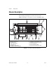
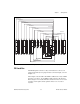
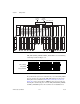
Figure 1-5. Distribution of PXI_CLK10, PXIe_CLK100, and PXIe_SYNC100
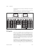
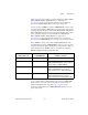
PXI_CLK10, PXIe_CLK100 and PXIe_SYNC100 have the default timing
relationship described in Figure 1-6.
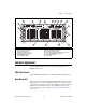
Figure 1-6. System Reference Clock Default Behavior
To synchronize the system to an external clock, you can drive PXI_CLK10
from an external source through the PXI_CLK10_IN pin on the System
Timing Slot. Refer to Table B-8, XP4 Connector Pinout for the System
Timing Slot, for the pinout. When a 10MHz clock is detected on this pin,
the backplane automatically phase-locks the PXI_CLK10, PXIe_CLK100,
and PXIe_SYNC100 signals to this external clock and distributes these
P2
P1
XP4
XP3
TP2
TP1
P2
P1
P2
P1
P2
P1
P1
P1
P1
XP4
XP3
XP4
XP3
XP4
XP3
XP4
XP3
XP4
XP3
XP4
XP3
XP4
XP3
P2
P1
P2
P1
P2
P1
P2
P1
P2
P1
XP4
XP3
XP2
XP1
P1
10 MHz
REF IN
10 MHz
REF OUT
PXI_CLK10_IN
1
8
9
10
PXIe_CLK100
PXIe_SYNC100
PXI_CLK10
7
H
11
HH
12
H
13
14
15
65
4
3
2
16 17 18
PXIe_CLK100
PXI_CLK10
PXIe_SYNC100
0123 45678 90123 45678 90123 45678 9