
Network Card User Manual
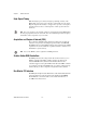
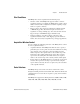
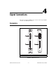
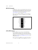
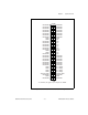
Table Of Contents
- IMAQ PCI/PXI-1428 User Manual
- Support
- Important Information
- Compliance
- Conventions
- Contents
- Chapter 1 Introduction
- Chapter 2 Installation
- Chapter 3 Hardware Overview
- Functional Overview
- Figure 3-1. IMAQ 1428 Block Diagram
- Camera Link and IMAQ 1428
- Data Transmission
- LUTs
- Multiple-Tap Data Formatter
- SDRAM
- Trigger Control and Mapping Circuitry
- High-Speed Timing
- Acquisition and Region of Interest (ROI)
- Scatter-Gather DMA Controllers
- Bus Master PCI Interface
- Start Conditions
- Acquisition Window Control
- Serial Interface
- Functional Overview
- Chapter 4 Signal Connections
- Appendix A Specifications
- Appendix B Cabling
- Appendix C Technical Support and Professional Services
- Glossary
- Index
Chapter 4 Signal Connections
IMAQ PCI/PXI-1428 User Manual 4-2 ni.com
MDR 26-Pin Connector
The MDR 26-pin connector provides reliable high-frequency transfer rates
between the camera and the acquisition device. To access this connector,
use a 3M Camera Link cable. For additional information on Camera Link
cables, including ordering information and cable lengths, refer to the
Camera Link Cables section of Appendix B, Cabling.
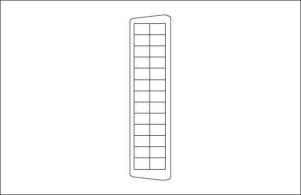
Figure 4-2 shows the IMAQ 1428 MDR 26-pin connector assignments.
Refer to Table 4-1 for a description of the MDR-26 and 68-pin VHDCI
signal connections.
Figure 4-2. MDR 26-Pin Connector Assignments
68-Pin VHDCI Connector
The 68-pin VHDCI connector connects to external digital I/O lines,
triggers, and medium configuration 8-bit × 4 mode. To access these
connections, build a custom cable or use an optional cable from National
Instruments. For information about building a custom cable for the 68-pin
VHDCI connector, refer to the 68-Pin VHDCI Cable Specifications section
of Appendix B, Cabling.
Figure 4-3 shows the 68-pin VHDCI connector pinout. Refer to Table 4-1
for a description of the MDR-26 and 68-pin VHDCI signal connections.
1
2
3
4
5
6
7
8
9
10
11
12
13
14
15
16
17
18
19
20
21
22
23
24
25
26
DGND
CC(4)–
CC(3)+
CC(2)–
CC(1)+
SerTFG+
SerTC–
X(3)+
XCLK+
X(2)+
X(1)+
X(0)+
DGND
DGND
CC(4)+
CC(3)–
CC(2)+
CC(1)–
SerTFG–
SerTC+
X(3)–
XCLK–
X(2)–
X(1)–
X(0)–
DGND