
Network Card User Manual
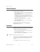
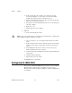
Table Of Contents
- IMAQ PCI/PXI-1428 User Manual
- Support
- Important Information
- Compliance
- Conventions
- Contents
- Chapter 1 Introduction
- Chapter 2 Installation
- Chapter 3 Hardware Overview
- Functional Overview
- Figure 3-1. IMAQ 1428 Block Diagram
- Camera Link and IMAQ 1428
- Data Transmission
- LUTs
- Multiple-Tap Data Formatter
- SDRAM
- Trigger Control and Mapping Circuitry
- High-Speed Timing
- Acquisition and Region of Interest (ROI)
- Scatter-Gather DMA Controllers
- Bus Master PCI Interface
- Start Conditions
- Acquisition Window Control
- Serial Interface
- Functional Overview
- Chapter 4 Signal Connections
- Appendix A Specifications
- Appendix B Cabling
- Appendix C Technical Support and Professional Services
- Glossary
- Index
© National Instruments Corporation 3-1 IMAQ PCI/PXI-1428 User Manual
3
Hardware Overview
This chapter provides an overview of IMAQ PCI/PXI-1428 hardware
functionality and explains the operations of the device’s functional units.
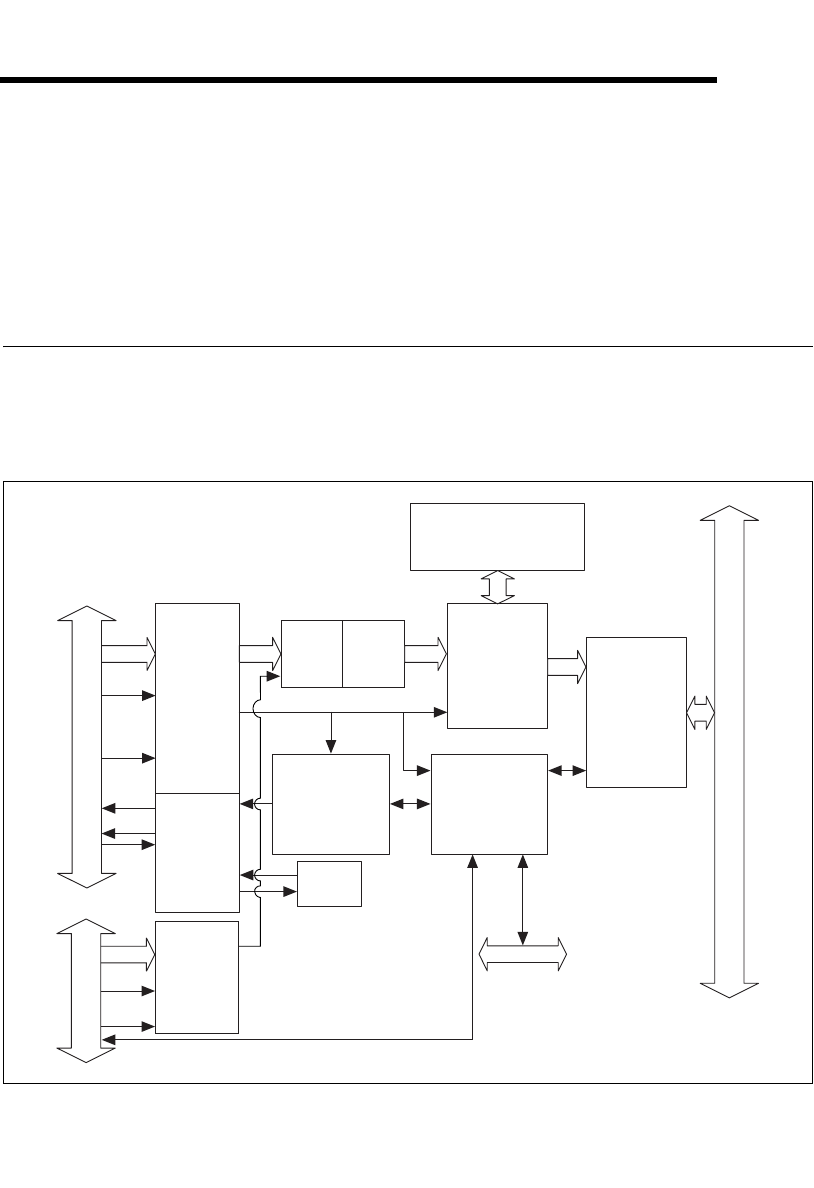
Functional Overview
The IMAQ 1428 features a flexible, high-speed data path optimized for
receiving and formatting video data from Camera Link cameras.
Figure 3-1 illustrates the key functional components of the IMAQ 1428.
Figure 3-1. IMAQ 1428 Block Diagram
Data
26-Pin MDR Connector
Channel
Link
Receiver
Enables
Pixel
Clock
Camera
Control
UART
PCI/PXI Bus
PCI/PXI Interface
and
Scatter-Gather
DMA Controllers
Data
IMAQ SDRAM
Interface
Synchronous Dynamic RAM
Advanced
Timing
Acquisition,
ROI, and Triggering
External Triggers
Pixel Clock and Camera Enables
RTSI Bus
LUT
LUT
Data
Data
Differential
Converter
68-Pin VHDCI
Serial
Control
Enables
Pixel
Clock
Channel
Link
Receiver
Data