
Network Card User Manual
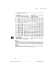
Table Of Contents
- PC-DIO-24 User Manual
- Contents
- About This Manual
- Chapter 1 Introduction
- Chapter 2 Configuration and Installation
- Chapter 3 Theory of Operation
- Chapter 4 Register-Level Programming
- Appendix A Specifications
- Appendix B I/O Connector
- Appendix C OKI 82C55A Data Sheet*
- Appendix D Customer Communication
- Glossary
- Index
- Figures
- Figure 1-1. The Relationship between the Programming Environment, NI-DAQ, and Your Hardware
- Figure 2-1. PC-DIO-24 Parts Locator Diagram
- Figure 2-2. Example Base I/O Address Switch Settings
- Figure 2-3. Jumper Settings–PC6, PC4, PC2, and N/C
- Figure 2-4. Interrupt Jumper Setting for IRQ5 (Factory Setting)
- Figure 2-5. Digital I/O Connector Pin Assignments
- Figure 3-1. PC-DIO-24 Block Diagram
- Figure 4-1. Control-Word Formats
- Figure B-1. PC-DIO-24 I/O Connector
- Tables
- Table 2-1. PC-DIO-24 Factory-Set Jumper and Switch Settings
- Table 2-2. Port C Signal Assignments
- Table 4-1. PC-DIO-24 Address Map
- Table 4-2. Port C Set/Reset Control Words
- Table 4-3. Mode 0 I/O Configurations
- Table 4-4. Interrupt Enable Signals for All Mode Combinations
- Table A-1. Maximum Average Transfer Rates for the PC-DIO-24
Index
PC-DIO-24 User Manual Index-2 © National Instruments Corporation
I
IBF signal
description (table), 2-8
mode 1 input timing, 2-9
mode 2 bidirectional timing, 2-11
IBFA bit, Port C, 4-8, 4-12
IBFB bit, Port C, 4-8
installation. See also configuration.
procedure for, 2-5
unpacking the PC-DIO-24, 1-6
INTE1 bit, Port C, 4-12
INTE2 bit, Port C, 4-13
INTEA bit, Port C, 4-8, 4-10
INTEB bit, Port C, 4-8, 4-10
interrupt control circuitry, 3-2
interrupt enable
factory settings (table), 2-1
jumper settings (figure), 2-4
setting, 2-4
interrupt handling, 4-15 to 4-16
interrupt enable signals for all mode
combinations (table), 4-16
recommended jumper settings for
W1, 4-16
interrupt level
factory settings (table), 2-1
jumper setting (figure), 2-4
settings, 2-4 to 2-5
interrupt programming examples, 4-14
to 4-15
INTR signal
description (table), 2-8
mode 1 input timing, 2-9
mode 1 output timing, 2-10
mode 2 bidirectional timing, 2-11
INTRA bit, Port C, 4-8, 4-10, 4-13
INTRB bit, Port C, 4-8, 4-10
I/O bit, Port C, 4-8, 4-10, 4-13
I/O connectors
digital I/O connector, 3-2
pin description (figure), 2-6, B-1
J
jumper and switch settings, 2-1 to 2-5
base I/O address settings, 2-1 to 2-3
factory settings, (table), 2-1
interrupt enable settings, 2-4
interrupt handling, 4-15 to 4-16
recommended jumper settings for
W1, 4-16
interrupt level settings, 2-4 to 2-5
L
LabVIEW and LabWindows/CVI
application software, 1-2
M
manual. See documentation.
mode 0 basic I/O, 4-5 to 4-7
configurations (table), 4-6
overview, 4-5
programming example, 4-6 to 4-7
purpose and use, 4-2
mode 1 input timing, 2-9
mode 1 output timing, 2-10
mode 1 strobed input, 4-7 to 4-9
control words written to CNFG register
(figures), 4-7
Port C pin assignments (figure), 4-8
Port C status-word bit definitions, 4-8
programming example, 4-9
purpose and use, 4-2
mode 1 strobed output, 4-9 to 4-11
control words written to CNFG register
(figure), 4-9 to 4-10
Port C pin assignments (figure), 4-11
Port C status-word bit definitions, 4-10
programming example, 4-11
purpose and use, 4-2
mode 2 bidirectional bus, 4-12 to 4-14
control word written to CNFG Register
(figure), 4-12
Port C pin assignments (figure), 4-13
Port C status-word bit definitions, 4-12
to 4-13
programming example, 4-13 to 4-14
purpose and use, 4-2
mode 2 bidirectional timing, 2-11