
Network Card User Manual
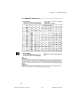
Table Of Contents
- PC-DIO-24 User Manual
- Contents
- About This Manual
- Chapter 1 Introduction
- Chapter 2 Configuration and Installation
- Chapter 3 Theory of Operation
- Chapter 4 Register-Level Programming
- Appendix A Specifications
- Appendix B I/O Connector
- Appendix C OKI 82C55A Data Sheet*
- Appendix D Customer Communication
- Glossary
- Index
- Figures
- Figure 1-1. The Relationship between the Programming Environment, NI-DAQ, and Your Hardware
- Figure 2-1. PC-DIO-24 Parts Locator Diagram
- Figure 2-2. Example Base I/O Address Switch Settings
- Figure 2-3. Jumper Settings–PC6, PC4, PC2, and N/C
- Figure 2-4. Interrupt Jumper Setting for IRQ5 (Factory Setting)
- Figure 2-5. Digital I/O Connector Pin Assignments
- Figure 3-1. PC-DIO-24 Block Diagram
- Figure 4-1. Control-Word Formats
- Figure B-1. PC-DIO-24 I/O Connector
- Tables
- Table 2-1. PC-DIO-24 Factory-Set Jumper and Switch Settings
- Table 2-2. Port C Signal Assignments
- Table 4-1. PC-DIO-24 Address Map
- Table 4-2. Port C Set/Reset Control Words
- Table 4-3. Mode 0 I/O Configurations
- Table 4-4. Interrupt Enable Signals for All Mode Combinations
- Table A-1. Maximum Average Transfer Rates for the PC-DIO-24

© National Instruments Corporation Glossary-1 PC-DIO-24 User Manual
Glossary
___________________________________________________
Prefix Meaning Value
µ- micro-
10
-6
m- milli-
10
-3
k- kilo-
10
3
M- mega-
10
6
° degrees
Ω ohms
% percent
A amperes
AWG American Wire Gauge
BCD binary-coded decimal
C Celsius
DMA direct memory access
hex hexadecimal
Hz hertz
in. inches
Iin input current
Iout output current
kbytes 1,024 bytes
LSB least significant bit
MB megabytes of memory
m meters
MSB most significant bit
PPI programmable peripheral interface
R
EXT
external resistance
s seconds
SSR solid-state relay
V volts
V
EXT
external volt
VDC volts direct current