
Network Card User Manual
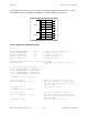
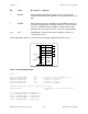

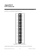
Table Of Contents
- PC-DIO-24 User Manual
- Contents
- About This Manual
- Chapter 1 Introduction
- Chapter 2 Configuration and Installation
- Chapter 3 Theory of Operation
- Chapter 4 Register-Level Programming
- Appendix A Specifications
- Appendix B I/O Connector
- Appendix C OKI 82C55A Data Sheet*
- Appendix D Customer Communication
- Glossary
- Index
- Figures
- Figure 1-1. The Relationship between the Programming Environment, NI-DAQ, and Your Hardware
- Figure 2-1. PC-DIO-24 Parts Locator Diagram
- Figure 2-2. Example Base I/O Address Switch Settings
- Figure 2-3. Jumper Settings–PC6, PC4, PC2, and N/C
- Figure 2-4. Interrupt Jumper Setting for IRQ5 (Factory Setting)
- Figure 2-5. Digital I/O Connector Pin Assignments
- Figure 3-1. PC-DIO-24 Block Diagram
- Figure 4-1. Control-Word Formats
- Figure B-1. PC-DIO-24 I/O Connector
- Tables
- Table 2-1. PC-DIO-24 Factory-Set Jumper and Switch Settings
- Table 2-2. Port C Signal Assignments
- Table 4-1. PC-DIO-24 Address Map
- Table 4-2. Port C Set/Reset Control Words
- Table 4-3. Mode 0 I/O Configurations
- Table 4-4. Interrupt Enable Signals for All Mode Combinations
- Table A-1. Maximum Average Transfer Rates for the PC-DIO-24

© National Instruments Corporation B-1 PC-DIO-24 User Manual
Appendix B
I/O Connector
This appendix describes the pinout and signal names for the I/O connector on the PC-DIO-24.
Figure B-1 shows the PC-DIO-24 digital I/O connector.
12
34
56
78
9
10
11 12
13
14
15 16
17 18
19 20
21 22
23 24
25 26
27 28
29 30
31 32
33 34
35 36
37 38
39 40
41 42
43 44
45 46
47 48
49 50
GND
GND
GND
GND
GND
GND
GND
GND
GND
GND
GND
GND
GND
GND
GND
GND
GND
GND
GND
GND
GND
GND
GND
GND
GND
PC7
PC6
PC5
PC4
PC3
PC2
PC1
PC0
PB7
PB6
PB5
PB4
PB3
PB2
PB1
PB0
PA 7
PA 6
PA 5
PA 4
PA 3
PA 2
PA 1
PA 0
+5V
Figure B-1. PC-DIO-24 I/O Connector
Detailed signal specifications are included in Chapter 2, Configuration and Installation.