
Network Card User Manual
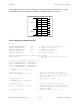
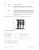
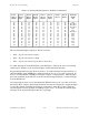

Table Of Contents
- PC-DIO-24 User Manual
- Contents
- About This Manual
- Chapter 1 Introduction
- Chapter 2 Configuration and Installation
- Chapter 3 Theory of Operation
- Chapter 4 Register-Level Programming
- Appendix A Specifications
- Appendix B I/O Connector
- Appendix C OKI 82C55A Data Sheet*
- Appendix D Customer Communication
- Glossary
- Index
- Figures
- Figure 1-1. The Relationship between the Programming Environment, NI-DAQ, and Your Hardware
- Figure 2-1. PC-DIO-24 Parts Locator Diagram
- Figure 2-2. Example Base I/O Address Switch Settings
- Figure 2-3. Jumper Settings–PC6, PC4, PC2, and N/C
- Figure 2-4. Interrupt Jumper Setting for IRQ5 (Factory Setting)
- Figure 2-5. Digital I/O Connector Pin Assignments
- Figure 3-1. PC-DIO-24 Block Diagram
- Figure 4-1. Control-Word Formats
- Figure B-1. PC-DIO-24 I/O Connector
- Tables
- Table 2-1. PC-DIO-24 Factory-Set Jumper and Switch Settings
- Table 2-2. Port C Signal Assignments
- Table 4-1. PC-DIO-24 Address Map
- Table 4-2. Port C Set/Reset Control Words
- Table 4-3. Mode 0 I/O Configurations
- Table 4-4. Interrupt Enable Signals for All Mode Combinations
- Table A-1. Maximum Average Transfer Rates for the PC-DIO-24
© National Instruments Corporation A-1 PC-DIO-24 User Manual
Appendix A
Specifications
This appendix lists the specifications for the PC-DIO-24 board. These specifications are typical at 25° C, unless
otherwise stated. The operating temperature range is 0° to 70° C.
Digital I/O
Number of channels .................................................... 24 I/O
Compatibility .............................................................. TTL
Absolute max voltage input rating .............................. -0.5 to +5.5 V with respect to GND
Handshaking................................................................ Requires 1 port
Power-on state............................................................. Configured as inputs
Data transfers .............................................................. Interrupts, programmed I/O
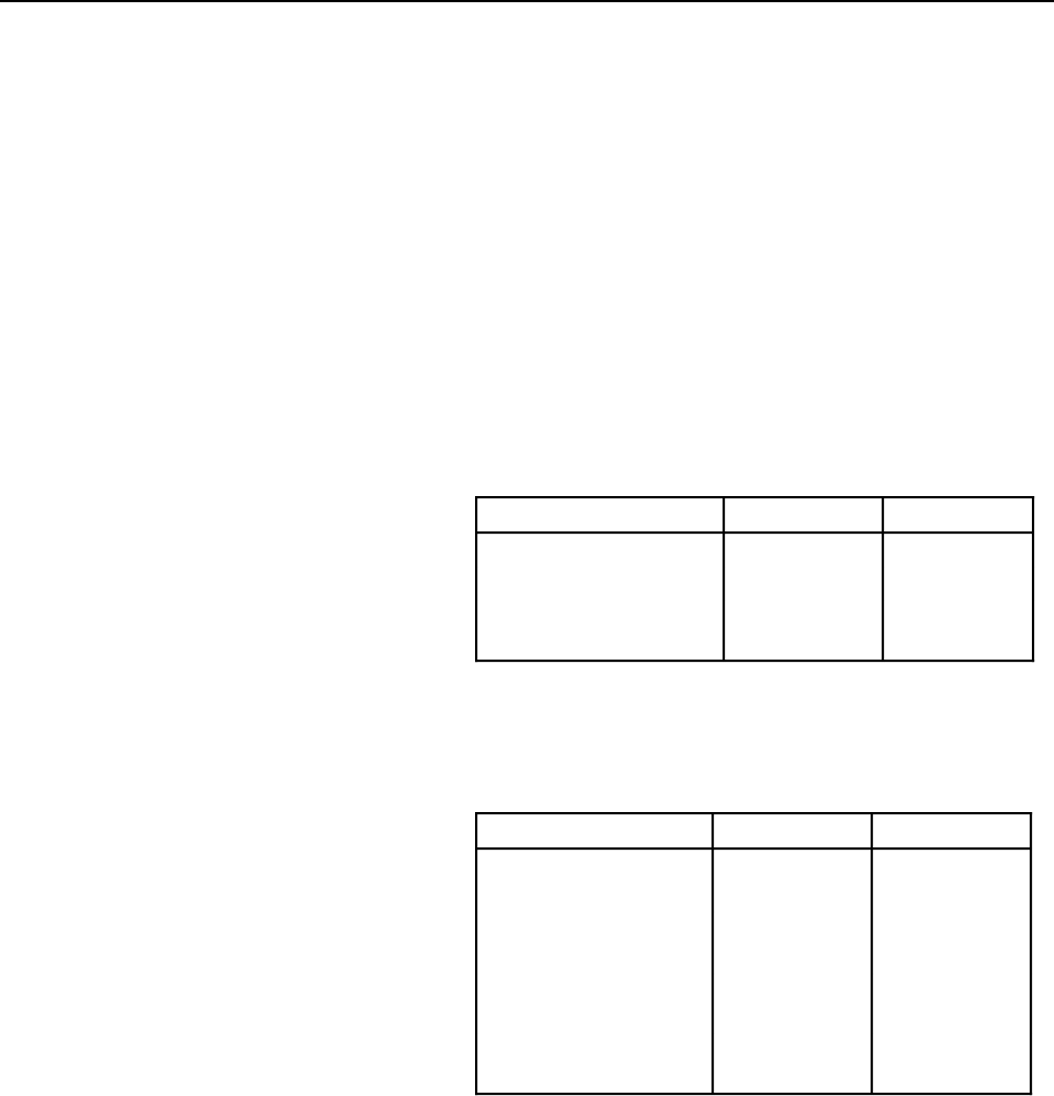
Digital Logic Levels
Input Signals
Odd-numbered pins 1–47......................................... Level
Min Max
Input logic high voltage 2.2 V 5.3 V
Input logic low voltage -0.3 V 0.8 V
Input current
(0 < V
in
< 5 V)
-1.0 µA 1.0 µA
Output Signals
Pin 49 (at +5 V)........................................................... 0.25 A max
Odd-numbered pins 1–47......................................... Level Min Max
Output high voltage
(I
out
= -2.5 mA) 3.7 V 5.0 V
Output low voltage
(I
out
= 2.5 mA) 0.0 V 0.4 V
Output current
(V
OL
= 0.5 V) 4 mA —
Output current
(V
OH
= 2.7 V) 4 mA —
Environment
Operating Temperature ............................................... 0° to 70° C
Storage Temperature ................................................... -55° to 150° C
Relative humidity ........................................................ 5% to 90% noncondensing