
Network Card User Manual
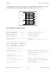
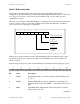
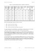

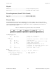
Table Of Contents
- PC-DIO-24 User Manual
- Contents
- About This Manual
- Chapter 1 Introduction
- Chapter 2 Configuration and Installation
- Chapter 3 Theory of Operation
- Chapter 4 Register-Level Programming
- Appendix A Specifications
- Appendix B I/O Connector
- Appendix C OKI 82C55A Data Sheet*
- Appendix D Customer Communication
- Glossary
- Index
- Figures
- Figure 1-1. The Relationship between the Programming Environment, NI-DAQ, and Your Hardware
- Figure 2-1. PC-DIO-24 Parts Locator Diagram
- Figure 2-2. Example Base I/O Address Switch Settings
- Figure 2-3. Jumper Settings–PC6, PC4, PC2, and N/C
- Figure 2-4. Interrupt Jumper Setting for IRQ5 (Factory Setting)
- Figure 2-5. Digital I/O Connector Pin Assignments
- Figure 3-1. PC-DIO-24 Block Diagram
- Figure 4-1. Control-Word Formats
- Figure B-1. PC-DIO-24 I/O Connector
- Tables
- Table 2-1. PC-DIO-24 Factory-Set Jumper and Switch Settings
- Table 2-2. Port C Signal Assignments
- Table 4-1. PC-DIO-24 Address Map
- Table 4-2. Port C Set/Reset Control Words
- Table 4-3. Mode 0 I/O Configurations
- Table 4-4. Interrupt Enable Signals for All Mode Combinations
- Table A-1. Maximum Average Transfer Rates for the PC-DIO-24
Chapter 4 Register-Level Programming
© National Instruments Corporation 4-11 PC-DIO-24 User Manual
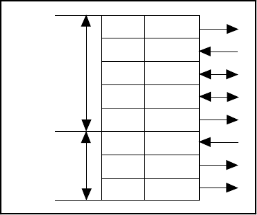
At the digital I/O connector, port C has the following pin assignments when in mode 1 output.
Notice that the status of ACKA* and ACKB* is not included when port C is read.
PC7
PC6
PC5
PC4
PC3
PC2
PC1
PC0
OBFA*
ACKA*
I/O
I/O
INTRA
ACKB*
OBFB*
INTRB
Group A
Group B
Mode 1 Output Programming Example
Main() {
#define BASE_ADDRESS 0x210 /* Board located at address 210. */
#define PORTAoffset 0x00 /* Offset for port A */
#define PORTBoffset 0x01 /* Offset for port B */
#define PORTCoffset 0x02 /* Offset for port C */
#define CNFGoffset 0x03 /* Offset for CNFG */
register unsigned int porta, portb, portc, cnfg;
char valread; /* Variable to store data read from a
port */
/* Calculate register addresses. */
porta = BASE_ADDRESS + PORTAoffset;
portb = BASE_ADDRESS + PORTBoffset;
portc = BASE_ADDRESS + PORTCoffset;
cnfg = BASE_ADDRESS + CNFGoffset;
/* EXAMPLE 1–port A output */
outp(cnfg,0xA0); /* Port A is an output in mode 1.*/
while (!(inp(portc) & 0x80)); /* Wait until OBFA* is set, indicating
that the data last written to port A
has been read.*/
outp(porta,0x12); /* Write data to port A. */
/* EXAMPLE 2–port B output */
outp(cnfg,0x84); /* Port B is an output in mode 1.*/
while (!(inp(portc) & 0x02)); /* Wait until OBFB* is set, indicating
that the data last written to port B
has been read.*/
outp(portb,0x34); /* Write the data to port B. */
}