
Network Card User Manual

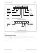
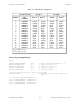
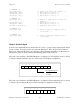
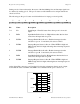
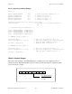

Table Of Contents
- PC-DIO-24 User Manual
- Contents
- About This Manual
- Chapter 1 Introduction
- Chapter 2 Configuration and Installation
- Chapter 3 Theory of Operation
- Chapter 4 Register-Level Programming
- Appendix A Specifications
- Appendix B I/O Connector
- Appendix C OKI 82C55A Data Sheet*
- Appendix D Customer Communication
- Glossary
- Index
- Figures
- Figure 1-1. The Relationship between the Programming Environment, NI-DAQ, and Your Hardware
- Figure 2-1. PC-DIO-24 Parts Locator Diagram
- Figure 2-2. Example Base I/O Address Switch Settings
- Figure 2-3. Jumper Settings–PC6, PC4, PC2, and N/C
- Figure 2-4. Interrupt Jumper Setting for IRQ5 (Factory Setting)
- Figure 2-5. Digital I/O Connector Pin Assignments
- Figure 3-1. PC-DIO-24 Block Diagram
- Figure 4-1. Control-Word Formats
- Figure B-1. PC-DIO-24 I/O Connector
- Tables
- Table 2-1. PC-DIO-24 Factory-Set Jumper and Switch Settings
- Table 2-2. Port C Signal Assignments
- Table 4-1. PC-DIO-24 Address Map
- Table 4-2. Port C Set/Reset Control Words
- Table 4-3. Mode 0 I/O Configurations
- Table 4-4. Interrupt Enable Signals for All Mode Combinations
- Table A-1. Maximum Average Transfer Rates for the PC-DIO-24
Chapter 4 Register-Level Programming
© National Instruments Corporation 4-7 PC-DIO-24 User Manual
/* EXAMPLE 1*/
outp(cnfg,0x80); /* Ports A, B, and C are outputs. */
outp(porta,0x12); /* Write data to port A. */
outp(portb,0x34); /* Write data to port B. */
outp(portc,0x56); /* Write data to port C. */
/* EXAMPLE 2*/
outp(cnfg,0x90); /* Port A is input; ports B and C are
outputs. */
outp(portb,0x22); /* Write data to port B. */
outp(portc,0x55); /* Write data to port C. */
valread = inp(porta); /* Read data from port A. */
/* EXAMPLE 3 */
outp(cnfg,0x82); /* Ports A and C are outputs; port B
is an input. */
/* EXAMPLE 4 */
outp(cnfg,0x89); /* Ports A and B are outputs; port C
is an input. */
}
Mode 1–Strobed Input
In mode 1, the digital I/O bits are divided into two groups—group A and group B. Each of these
groups contains one 8-bit port and one 4-bit control/data port. The 8-bit port can be either an
input or an output, and the 4-bit port is used for control and status information for the 8-bit port.
The transfer of data is synchronized by handshaking signals in the 4-bit port.
The control word written to the CNFG Register to configure port A for input in mode 1 is shown
as follows. Bits PC6 and PC7 of port C can be used as extra input or output lines.
1 0 1 1 1/0 XXX
7654 3210
1 = input
0 = output
Port C bits PC6 and PC7
The control word written to the CNFG Register to configure port B for input in mode 1 is shown
as follows. Notice that port B does not have extra input or output lines from port C.
1 X X X X11X
76543210