
Network Card User Manual

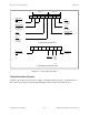
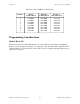
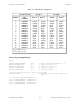

Table Of Contents
- PC-DIO-24 User Manual
- Contents
- About This Manual
- Chapter 1 Introduction
- Chapter 2 Configuration and Installation
- Chapter 3 Theory of Operation
- Chapter 4 Register-Level Programming
- Appendix A Specifications
- Appendix B I/O Connector
- Appendix C OKI 82C55A Data Sheet*
- Appendix D Customer Communication
- Glossary
- Index
- Figures
- Figure 1-1. The Relationship between the Programming Environment, NI-DAQ, and Your Hardware
- Figure 2-1. PC-DIO-24 Parts Locator Diagram
- Figure 2-2. Example Base I/O Address Switch Settings
- Figure 2-3. Jumper Settings–PC6, PC4, PC2, and N/C
- Figure 2-4. Interrupt Jumper Setting for IRQ5 (Factory Setting)
- Figure 2-5. Digital I/O Connector Pin Assignments
- Figure 3-1. PC-DIO-24 Block Diagram
- Figure 4-1. Control-Word Formats
- Figure B-1. PC-DIO-24 I/O Connector
- Tables
- Table 2-1. PC-DIO-24 Factory-Set Jumper and Switch Settings
- Table 2-2. Port C Signal Assignments
- Table 4-1. PC-DIO-24 Address Map
- Table 4-2. Port C Set/Reset Control Words
- Table 4-3. Mode 0 I/O Configurations
- Table 4-4. Interrupt Enable Signals for All Mode Combinations
- Table A-1. Maximum Average Transfer Rates for the PC-DIO-24

Register-Level Programming Chapter 4
PC-DIO-24 User Manual 4-6 © National Instruments Corporation
Table 4-3. Mode 0 I/O Configurations
Control Word Group A Group B
Number Bit Port A Port C
1
Port B Port C
2
76543210
0 10000000 Output Output Output Output
1 10000001 Output Output Output Input
2 10000010 Output Output Input Output
3 10000011 Output Output Input Input
4 10001000 Output Input Output Output
5 10001001 Output Input Output Input
6 10001010 Output Input Input Output
7 10001011 Output Input Input Input
8 10010000 Input Output Output Output
9 10010001 Input Output Output Input
10 10010010 Input Output Input Output
11 10010011 Input Output Input Input
12 10011000 Input Input Output Output
13 10011001 Input Input Output Input
14 10011010 Input Input Input Output
15 10011011 Input Input Input Input
1
Upper nibble of port C
2
Lower nibble of port C
Mode 0 Programming Example
Main() {
#define BASE_ADDRESS 0x210 /* Board located at address 210 */
#define PORTAoffset 0x00 /* Offset for port A */
#define PORTBoffset 0x01 /* Offset for port B */
#define PORTCoffset 0x02 /* Offset for port C */
#define CNFGoffset 0x03 /* Offset for CNFG */
register unsigned int porta, portb, portc, cnfg;
char valread; /* Variable to store data read from a
port */
/* Calculate register addresses. */
porta = BASE_ADDRESS + PORTAoffset;
portb = BASE_ADDRESS + PORTBoffset;
portc = BASE_ADDRESS + PORTCoffset;
cnfg = BASE_ADDRESS + CNFGoffset;