
Network Card User Manual
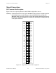
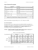
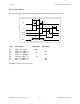
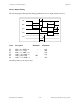
Table Of Contents
- PC-DIO-24 User Manual
- Contents
- About This Manual
- Chapter 1 Introduction
- Chapter 2 Configuration and Installation
- Chapter 3 Theory of Operation
- Chapter 4 Register-Level Programming
- Appendix A Specifications
- Appendix B I/O Connector
- Appendix C OKI 82C55A Data Sheet*
- Appendix D Customer Communication
- Glossary
- Index
- Figures
- Figure 1-1. The Relationship between the Programming Environment, NI-DAQ, and Your Hardware
- Figure 2-1. PC-DIO-24 Parts Locator Diagram
- Figure 2-2. Example Base I/O Address Switch Settings
- Figure 2-3. Jumper Settings–PC6, PC4, PC2, and N/C
- Figure 2-4. Interrupt Jumper Setting for IRQ5 (Factory Setting)
- Figure 2-5. Digital I/O Connector Pin Assignments
- Figure 3-1. PC-DIO-24 Block Diagram
- Figure 4-1. Control-Word Formats
- Figure B-1. PC-DIO-24 I/O Connector
- Tables
- Table 2-1. PC-DIO-24 Factory-Set Jumper and Switch Settings
- Table 2-2. Port C Signal Assignments
- Table 4-1. PC-DIO-24 Address Map
- Table 4-2. Port C Set/Reset Control Words
- Table 4-3. Mode 0 I/O Configurations
- Table 4-4. Interrupt Enable Signals for All Mode Combinations
- Table A-1. Maximum Average Transfer Rates for the PC-DIO-24
Configuration and Installation Chapter 2
PC-DIO-24 User Manual 2-10 © National Instruments Corporation
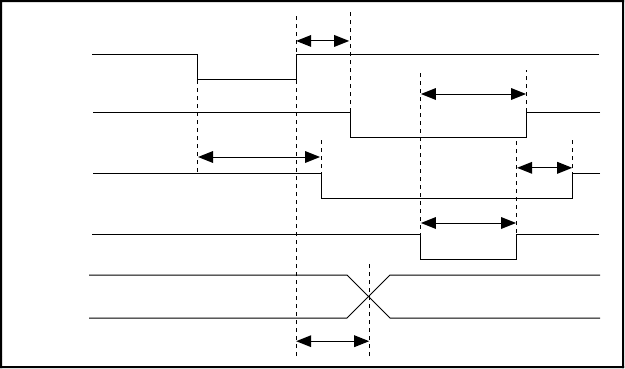
Mode 1 Output Timing
The following figure illustrates the timing specifications for an output transfer in mode 1.
T2
T3
WR*
OBF*
INTR
DATA
T4
T6
T5
ACK*
T1
Name Description Minimum Maximum
T1 WR* = 0 to INTR = 0 – 250
T2 WR* = 1 to output – 200
T3 WR* = 1 to OBF* = 0 – 150
T4 ACK* = 0 to OBF* = 1 – 150
T5 ACK* pulse width 100 –
T6 ACK* = 1 to INTR = 1 – 150
All timing values are in nanoseconds.