
Network Card User Manual
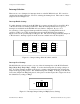
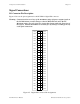
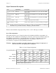
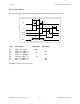
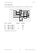
Table Of Contents
- PC-DIO-24 User Manual
- Contents
- About This Manual
- Chapter 1 Introduction
- Chapter 2 Configuration and Installation
- Chapter 3 Theory of Operation
- Chapter 4 Register-Level Programming
- Appendix A Specifications
- Appendix B I/O Connector
- Appendix C OKI 82C55A Data Sheet*
- Appendix D Customer Communication
- Glossary
- Index
- Figures
- Figure 1-1. The Relationship between the Programming Environment, NI-DAQ, and Your Hardware
- Figure 2-1. PC-DIO-24 Parts Locator Diagram
- Figure 2-2. Example Base I/O Address Switch Settings
- Figure 2-3. Jumper Settings–PC6, PC4, PC2, and N/C
- Figure 2-4. Interrupt Jumper Setting for IRQ5 (Factory Setting)
- Figure 2-5. Digital I/O Connector Pin Assignments
- Figure 3-1. PC-DIO-24 Block Diagram
- Figure 4-1. Control-Word Formats
- Figure B-1. PC-DIO-24 I/O Connector
- Tables
- Table 2-1. PC-DIO-24 Factory-Set Jumper and Switch Settings
- Table 2-2. Port C Signal Assignments
- Table 4-1. PC-DIO-24 Address Map
- Table 4-2. Port C Set/Reset Control Words
- Table 4-3. Mode 0 I/O Configurations
- Table 4-4. Interrupt Enable Signals for All Mode Combinations
- Table A-1. Maximum Average Transfer Rates for the PC-DIO-24

Chapter 2 Configuration and Installation
© National Instruments Corporation 2-7 PC-DIO-24 User Manual
Signal Connection Descriptions
Pin Signal Name Description
1, 3, 5, 7, 9, 11, 13,
15
PC<7..0> Port C—Bidirectional data lines for port C. PC7 is the MSB,
PC0 the LSB.
17, 19, 21, 23, 25,
27, 29, 31
PB<7..0> Port B—Bidirectional data lines for port B. PB7 is the MSB,
PB0 the LSB.
33, 35, 37, 39, 41,
43, 45, 47
PA<7..0> Port A—Bidirectional data lines for port B. PA7 is the MSB,
PA0 the LSB.
49 (see note below) +5 V +5 Volts—This pin provides +5 VDC.
All even-numbered
pins
GND Ground—These signals are connected to the PC ground signal.
Note: Pin 49 is connected to the +5 V PC power supply via a 1 A fuse. A replacement fuse is available from
Allied Electronics, part number 845-2007, or Littelfuse, part number 251001.
The absolute maximum voltage input rating is -0.5 to +5.5 V with respect to GND.
Port C Pin Assignments
The signals assigned to port C depend on the mode in which the 82C55A is programmed. In
mode 0, port C is considered two 4-bit I/O ports. In modes 1 and 2, port C is used for status and
handshaking signals with two or three I/O bits mixed in. Table 2-2 summarizes the signal
assignments of port C for each programmable mode. See Chapter 4, Register-Level
Programming, for register-level programming information.
Warning: During programming, note that each time a port is configured, output ports A
and C are reset to 0, and output port B is undefined.
Table 2-2. Port C Signal Assignments
Programming Mode Group A Group B
PC7 PC6 PC5 PC4 PC3 PC2 PC1 PC0
Mode 0
I/O I/O I/O I/O I/O I/O I/O I/O
Mode 1 Input
I/O I/O IBF
A
STB
A
* INTR
A
STB
B
* IBFB
B
INTR
B
Mode 1 Output
OBF
A
* ACK
A
* I/O I/O INTR
A
ACK
B
* OBF
B
* INTR
B
Mode 2
OBF
A
* ACK
A
* IBF
A
STB
A
* INTR
A
I/O I/O I/O
* Indicates that the signal is active low.