
Network Card User Manual
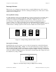
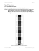
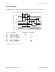
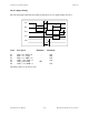
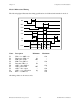
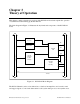
Table Of Contents
- PC-DIO-24 User Manual
- Contents
- About This Manual
- Chapter 1 Introduction
- Chapter 2 Configuration and Installation
- Chapter 3 Theory of Operation
- Chapter 4 Register-Level Programming
- Appendix A Specifications
- Appendix B I/O Connector
- Appendix C OKI 82C55A Data Sheet*
- Appendix D Customer Communication
- Glossary
- Index
- Figures
- Figure 1-1. The Relationship between the Programming Environment, NI-DAQ, and Your Hardware
- Figure 2-1. PC-DIO-24 Parts Locator Diagram
- Figure 2-2. Example Base I/O Address Switch Settings
- Figure 2-3. Jumper Settings–PC6, PC4, PC2, and N/C
- Figure 2-4. Interrupt Jumper Setting for IRQ5 (Factory Setting)
- Figure 2-5. Digital I/O Connector Pin Assignments
- Figure 3-1. PC-DIO-24 Block Diagram
- Figure 4-1. Control-Word Formats
- Figure B-1. PC-DIO-24 I/O Connector
- Tables
- Table 2-1. PC-DIO-24 Factory-Set Jumper and Switch Settings
- Table 2-2. Port C Signal Assignments
- Table 4-1. PC-DIO-24 Address Map
- Table 4-2. Port C Set/Reset Control Words
- Table 4-3. Mode 0 I/O Configurations
- Table 4-4. Interrupt Enable Signals for All Mode Combinations
- Table A-1. Maximum Average Transfer Rates for the PC-DIO-24
Configuration and Installation Chapter 2
PC-DIO-24 User Manual 2-6 © National Instruments Corporation
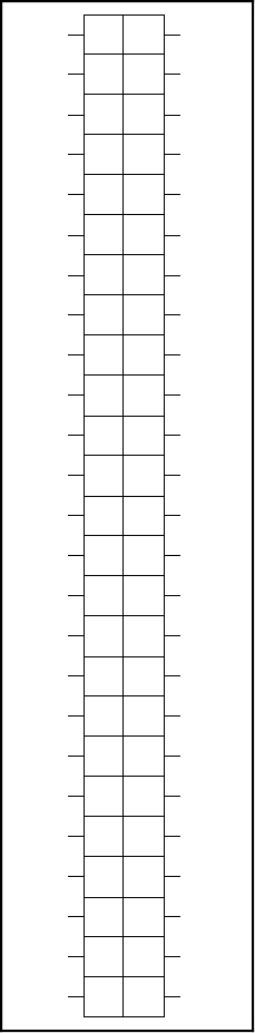
Signal Connections
I/O Connector Pin Description
Figure 2-5 shows the pin assignments for the PC-DIO-24 digital I/O connector.
Warning: Connections that exceed any of the maximum ratings of input or output signals on
the PC-DIO-24 may result in damage to the PC-DIO-24 board and to the PC.
Maximum ratings for each signal are given in this chapter under the discussion of
that signal. National Instruments is not liable for any damages resulting from any
such signal connections.
12
34
56
78
9
10
11 12
13
14
15 16
17 18
19 20
21 22
23 24
25 26
27 28
29 30
31 32
33 34
35 36
37 38
39 40
41 42
43 44
45 46
47 48
49 50
GND
GND
GND
GND
GND
GND
GND
GND
GND
GND
GND
GND
GND
GND
GND
GND
GND
GND
GND
GND
GND
GND
GND
GND
GND
PC7
PC6
PC5
PC4
PC3
PC2
PC1
PC0
PB7
PB6
PB5
PB4
PB3
PB2
PB1
PB0
PA 7
PA 6
PA 5
PA 4
PA 3
PA 2
PA 1
PA 0
+5V
Figure 2-5. Digital I/O Connector Pin Assignments